Yao N. Focused Ion Beam Systems: Basics and Applications
Подождите немного. Документ загружается.

such defects are observed (Figure 9.7(b)). From the TEM image quality of
the sample thinned at 10 kV, it is again obvious that the sample can be cleanly
and smoothly thinned using a lower energy ion beam. These experimental
results demonstrate well the importance of choosing a low energy ion beam
for final milling in TEM sample preparation.
But these data does not tell us how deep samples will get damaged. When
studying the surface region of a sample, it is worth knowing the depth of
damage on your sample. A measurement of the thickness of the damage that
occurred on a single crystal Si is shown in Figure 9.8 . The samples were final
milled at 30 kV and 10 kV, and the thickness of the amorphous layers formed
as the result of ion beam irradiation damage are 21 nm and 8 nm, respec-
tively. The results of the measurement reveal that the damage depth is almost
proportional to the energy of the ion beam employed in the final milling. In
case you still have a damage problem, even after reducing the ion beam
energy to the practical limit of the FIB system, additional thinning by a
conventional method, e.g., Ar ion milling, will work.
9.3 High-resolution TEM image observation of
FIB prepared samples
Although a certain rate of damage occurs on the cross-sectioned surfaces of
an FIB milled thin sample, high-resolution TEM image observation is pos-
sible in most cases if the sample is prepared properly. Figure 9.9 shows a
high-resolution TEM image of a semiconductor device. The sample was
Si
C
W
21nm
30 kV
50nm
50nm
a
8nm
10 kV
b
Si
C
W
50nm
50nm
Si
C
W
21nm
30 kV
50nm
50nm
a
8nm
10 kV
b
Si
C
W
50nm
50nm
Si
C
W
21 nm
30 kV
50 nm
(a)
8 nm
10 kV
(b)
Si
C
W
50 nm
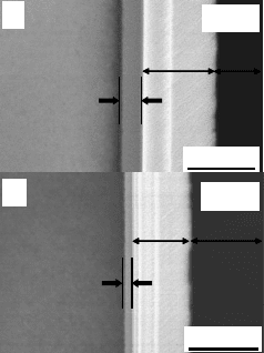
Figure 9.8 Cross-sectional dark-field STEM images of amorphous layers
formed during FIB milling. 21 nm and 8 nm thick amorphous layers were
formed at (a) 30 kV and (b) 10 kV, respectively. C and W in the photographs
indicate carbon and tungsten deposition layers.
Focused ion beam systems258
thinned to a thickness of 80 nm at 10 kV. Although it has a 16 nm thick
amorphous layer on both surfaces, as demonstrated in the previous section,
crystal lattice fringes obtained with the electron beam incident along the (110)
plane of the silicon and individual Si atoms at the interface between the Si
substrate and the silicon oxide above it are clearly observed. This kind of
image quality, however, only became possible after the FIB milling technique
at low energy, e.g., 10 kV, was routinely adopted for TEM sample prepara-
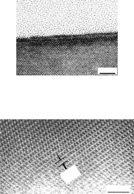
tion. Figure 9.10 shows a high-resolution TEM image of hydroxyapatite,
which is one of the most sensitive materials to electron beam irradiation, and
5 nm
Figure 9.9 Cross-sectional high-resolution TEM image of an Si substrate
and silicon oxide layer of a semiconductor device. The sample was thinned
at 10 kV to the thickness of 80 nm. The atomic array at the top of the
substrate and the fine structure of the amorphous silicon oxide layer can be
clearly observed.
3
nm
(100)
0.817 nm
Figure 9.10 High-resolution TEM image of a hydroxyapatite crystal of
human tooth. Lattice fringes of (100) crystal plane with a separation
distance of 0.817 nm can be clearly observed.
In-situ sample manipulation and imaging 259
therefore considered to be difficult to thin using the FIB technique without
causing damage. However, crystal lattice fringes of the (100) plane with a
distance of 0.817 nm and other fine structures can be clearly observed.
From the image, it is evident that the quality of the high-resolution TEM
image does not suffer from the damage that occurred during the FIB milling.
9.4 FIB capability in TEM sample preparation
Recent developments and improvements of the FIB techniques for TEM
sample preparation have enabled us to observe fine structures of many
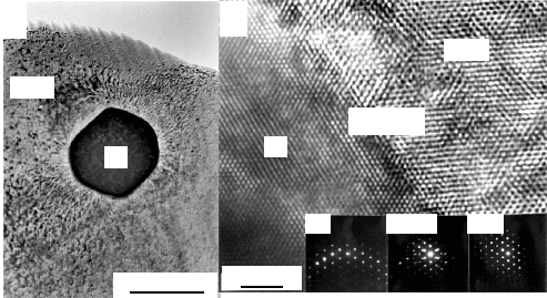
composite materials [12–13]. Figure 9.11 shows a low-magnification cross-
sectional TEM image of a tungsten (W) fiber embedded in zirconia (ZrO
2
)
(Figure 9. 11 (a)) and a high-resolution TEM image with a nano-probe electron
diffraction pattern of the interface (Figure 9.11(b)). Since the material is a very
hard metal and ceramic composite material, it was impossible to prepare an
adequate TEM sample for the study of the interface between the two
materials. As is shown here in the sample prepared by the FIB technique,
however, we can observe the whole structure of the cross section of the W
fiber and the interface structure of the W–ZrO
2
interface at an atomic
resolution.
The capability of the FIB technique in practice is greater than expected.
Figure 9.12 shows a TEM image of a toner particle thinned by the FIB
technique. The sample was coated with an FIB assisted W deposition layer
prior to the thinning process and thinned by FIB milling at an acceleration
voltage of 30 kV. Although the material has a very low melting point and was
therefore considered impossible to thin using the FIB technique, the original
W
500nm
a
b
interface
W
2 n m
inte rface
W
ZrO
2
W
500 nm
(a)
(b)
Interface
W
ZrO
2
2 nm
ZrO
2
Interface
W
Figure 9.11 (a) Low-magnification TEM image of a cross-sectioned W fiber
embedded in ZrO
2
and (b) a high-resolution TEM image of the interface
with the inser tion of electron diffraction patterns from the interface.
Focused ion beam systems260
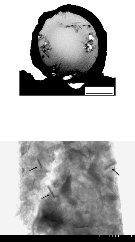
shape of the particle and its internal structure are well preserved. So far the
thin sectioning of this kind of material with a very low melting point has only
been possible with a cryo-sectioning technique that requires special training.
Figure 9.13 shows a STEM image of a thin section of paraffin embedded
human lung tissue which was prepared for characterization of inhaled
mineral fibers. The sample was extracted from the paraffin block of tissue
and thinned to a thickness of 5 mm at an acceleration voltage of 30 kV.
Mineral fibers in the tissue (indicated by the arrows) can be clearly observed.
2 m
Figure 9.12 Bright field STEM image of a toner particle thinned at 40 kV.
The toner is covered with an FIB assisted W deposition layer. The original
shape of the toner particle and the inside structures are well preserved.
3.00m
HD-2000 200kV ×10.0k TE
Figure 9.13 STEM image of a paraffin embedded human lung. A small piece
of the sample was extracted and thinned at 30 kV.
In-situ sample manipulation and imaging 261
From these images it can be said that the FIB technique has made TEM
sample preparation of the materials of low-melting point much easier than
before.
9.5 TEM sample preparation from a specific site
One of the advantages of the FIB technique compared with other conven-
tional TEM sample preparation techniques is the excellent positional accu-
racy in setting the area to be thinned. However, because structures are
becoming smaller and more complicated, TEM sample preparation from
specific sites in state of the art materials such as semiconductor devices is no
more easy than it was in the past. Various approaches to improve the posi-
tional accuracy are being developed and some have already been put to
effective use. One of the most reliable systems used for this purpose is a
dedicated FIB-STEM system. The system has a compatible sample holder so
that sample preparation in the FIB system and its observation in the STEM
are possible without reloading the sample [14].
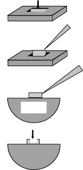
Figure 9.14 shows the procedure for TEM sample preparation from a
specific site using the FIB-STEM system. In this method, the sample is milled
to a thickness of 3–5 mm and transferred to the STEM unit to observe STEM
and SEM images. The presence of the site in the sample can be confirmed by
the STEM observation and the position of the site can be assured by the
SEM observation three dimensionally. The sample is then transferred back to
(a)
Ga+
3–5m
<0.1m
(b)
e
–
e
–
e
–
(d)
(c)
Figure 9.14 Pr ocedure for TEM sample preparation from a specific site.
(a) The sample is milled to a thickness of 3–5 mm. Then transferred to the
STEM unit for (b) STEM and (c) SEM observation to find the site to be
thinned. (d) Finally, transferred to the FIB system to make a <0.1 mm thick
sample from the specific site.
Focused ion beam systems262
the FIB system to make a TEM sample exactly from the site to be char-
acterized. In this method, we use STEM for the observation of interior
structures so that we can minimize unwanted sample damage caused by Ga
ion beam irradiation. This is an important advantage when the structural
analysis of a specific site at atomic level resolution is required.
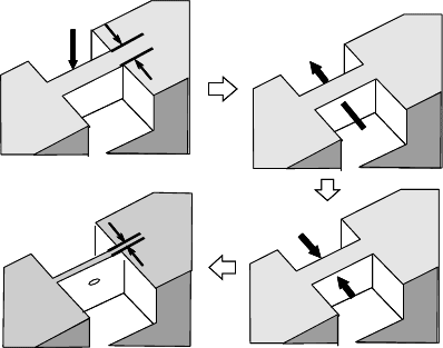
9.5.1 FIB lift-out technique
The FIB lift-out technique was developed for lifting out a thinned sample
directly from a bulky sample [ 15–16]. The general flow chart of the lift-out
technique is shown in Figure 9.15. First, the sample is inserted into the FIB
system and the surrounding area of the site to be characterized is trench
milled (Figure 9.15(a)) and the site is thinned to electron-transparent thick-
ness (100 nm or less) (Figure 9.15(b)). The sample is then transferred to the
stage of a light microscope and the thinned sample is lifted out using a glass
rod (Figure 9.15(c)), and deposited onto a carbon coated TEM grid (Figure
9.15(d)). The technique may be applied to most of the substances used in
industrial materials. Although the procedure is simple, the samples prepared
by the technique have a clean surface and uniform thickness so that even
atomic level high-resolution TEM images can be observed. Since the tech-
nique does not require any mechanical polishing or dicing prior to the FIB
milling, the time required for the whole process is much shorter than that
required for conventional FIB techniques.
Probe
TEM
g
rid
(a)
(b)
(c)
(d)
Ga
+
Ga
+
Figure 9.15 General flow chart of a lift-out technique. (a) Trench mill the
surrounding area, (b) thin the site to be characterized, (c) lift the thinned
sample out, (d) deposit the sample on a carbon coated TEM grid.
In-situ sample manipulation and imaging 263
This is an advantage when many samples need to be prepared in a short
time. However, since a glass rod is used for lifting and mounting the sample,
some experience is required to achieve a good success rate, and a better way
to mount and align the sample is desired. Figure 9.16(a) shows a trench
milled and cross-sectioned area, and the sample mounted on a carbon coated
TEM grid is shown in Figure 9.16(b).
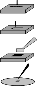
9.5.2 FIB micro-sampling technique
This technique has also been developed for TEM sample preparation of a
specific site. The general flow chart of the FIB micro-sampling technique is
shown in Figure 9.17. First, the area surrounding the site to be characterized is
trench milled (Figure 9. 17 ( a )) . S ec on d, c r o s s s ec ti on t h e s it e a n d p i ck u p a
sample piece (Figure 9.1 7(b)). Next the sample is mounted on a carrier (Figure
9.17(c)), and thinned using FIB milling (Figure 9.17(d)). All of the steps above
are accomplished under vacuum in the FIB system. Since the sample is
manipulated by an elaborate mechanical probe and bonded by FIB assisted
deposition, the success rate is very high and therefore it is used as one of the
standard TEM sampling techniques in a wide range of materials [17–18].
The technique has the following unique features:
1. No mech anical pre-th inning such as dicing or fracturi ng is necessa ry.
2. It is capab le of both cross- sectional and plan-v iew TEM micro -sampli ng.
3. Plan-vi ew TEM micr o-sampling from identical areas in cross- sectional TEM view
are pos sible, an d vice versa.
4. It is well suited for TEM obs ervation of magn etic mate rials because the sampl e is
so small and the influence of the magnetic fie ld from the sample is negligibly
small.
5. Good results in quantitative EDX analysis can be expected because the sample is
so small and any material may be used as the sample carrier.
10um10um
10 m
(a)
(b)
Figure 9.16 Trench milled area and a thinned sample (a) and the sample
mounted on a carbon coated TEM grid (b).
Focused ion beam systems264
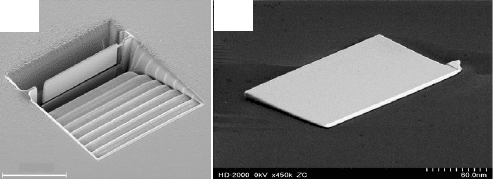
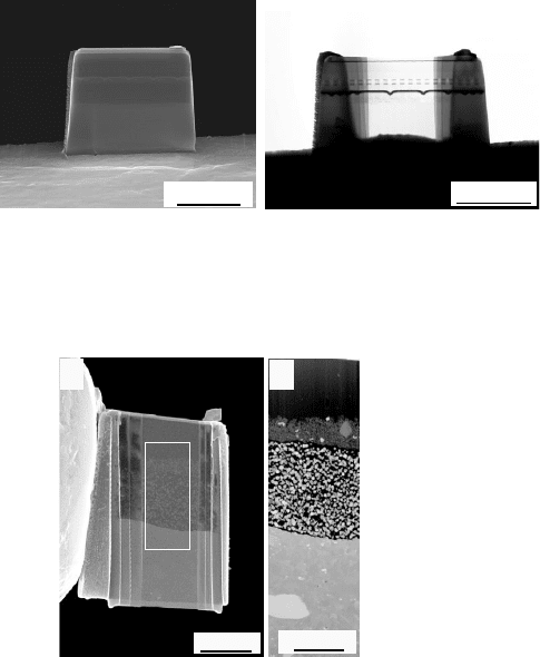
Fi gu r e 9.18(a) s hows a micro-sample mounted on a carrier and Fi gure 9.18(b)
shows a sample after thinning. A typical size of the micro-sample is 10–20 mm
wide, 10–15 m m high, and 2–5 m m thick. The technique can be applied to a
wide range of materials including semiconductor materials, metals, ceramics,
polymers, and various kinds of composite materials.
Figure 9.19(a) shows a micro-sample of a coating of a beverage can and
Figure 9.19(b) shows a magnified STEM image of a framed area in (a). The
layers composed of an anti-bacterial coating, the printed layer and a pro-
tective layer of the can are thinned uniformly. Although the sample was
extracted upward by a mechanical probe bonded to the surface of the micro-
sample, no damage such as micro-cracking occurred at the interface between
Al and coating. As is demonstrated here, the adhesive force of the FIB
assisted metal deposition layer is strong enough to extract and carry the
micro-sample, even if the surface is covered with a nonconductive and plastic
polymer.
9.6 Summary and future prospects
Nanotechnology is based on well-designed and manufactured nanomaterials.
In the characterization of the nanomaterials, the structural and composi-
tional analyses of nanometer-scaled areas is essential. TEM is one of the
carrier
probe
Probe
(a)
(b)
(c)
(d)
Ga
Ga
+
+
Ga
Ga
+
carrier
Carrier
Ga
Ga
+
Figure 9.17 General flow chart of an FIB micro-sampling technique.
(a) Trench mill the surrounding area, (b) cross-section and pick up using
a mechanical probe, (c) mount on a carrier, (d) Thin the site to be
characterized.
In-situ sample manipulation and imaging 265
most used instruments in this characterization, and sample preparation for
TEM observation is the first and most important thing to do. Among several
TEM sample preparation methods in use, the FIB technique is distinguished
as the best method to prepare a TEM sample from a specific site. In fact, the
success rate in failure analysis of semiconductor devices using TEM
improved significantly after the FIB technique was applied. In materials
characterization, however, new results bring new requirements, and the
requirements of the materials scientist are growing steadily more challenging.
Actually, quite a few of the latest requirements coming from high-tech
industry concern the capability of the single FIB technique, especially in
positional accuracy. The combination of FIB and STEM systems, however,
could improve the positional accuracy in TEM sample preparation drasti-
cally. In this method, electrons instead of Ga ions, are used for observation
of the sample; consequent damage during searching the site or positioning
the milling area is much less than that of conventional FIB technique.
(a)
(b)
10 m 10 m
Figure 9.18 FIB micro-sample of semiconductor device mounted on a
carrier (a) and a thinned micro-sample (b).
Protective W
layer
Print layer
Anti-bacterial
coating
Al
(a)
(b)
10
µ
m
5
µ
m
Figure 9.19 (a) SEM image of a micro-sample of a coating of a beverage can
and (b) a dark field STEM image of the framed area in (a).
Focused ion beam systems266
In materials science, the importance of TEM investigation is constantly
increasing and most investigations require site-specific sample preparation.
The future will throw up many challenges in this world, and FIB will
continue to be the best solution in the future as well.
References
[1] E. C. G. Kirk, D. A. Williams and H. Ahmed. Microsc. Semicond. Mater. Sci.,
Inst. Phys. Conf. Ser., 100 (1989) 501–6.
[2] T. Ishitani, H. Tsuboi, T. Yaguchi and H. Koike. J. Electron Microsc., 4 (1994),
322–6.
[3] A. R. Neureuther, C. Y. Liu and C. H. Ting. J. Vac. Sci. Technol., 16 (1979) ,
1767–71.
[4] Y. Kitano, Y. Fujikawa, T. Kamino, et al. J. Electron Microsc., 44 (1995),
410–13.
[5] Y. Kitano, Y. Fujikawa, T. Kamino, et al. J. Electron Microsc., 44 (1995),
376–83.
[6] T. Ishitani and T. Ohnishi. J. Vac. Sci. Technol. A, 9 (1991) , 3084–9.
[7] D. W. Susnitzky and K. D. Johnson. Proc. Microsc. Microanal., 4 (1998), 636–7.
[8] J. Melngailis. Electron Beam, X-ray and Ion-beam Submicrometer Lithographies
for Manufacturing, Proc. SPIE, 1465 (1991), 36–49.
[9] T. Ishitani. Jpn. J. Appl. Phys., 34 (1995), 3303–6.
[10] T. Ishitani, H. Koike, T. Yaguchi and T. Kamino. J. Vac. Sci. Technol. B, 16
(1998), 1907–13.
[11] W. Hauffe. Top. Appl. Phys., 64 (1991), 305–38.
[12] H. Saka, T. Kato, M. H. Hong, et al. Proc. Galvatech., (1995).
[13] H. Saka. The 10th Int. Symp. on Advanced Materials, (Tsukuba, Japan, 2003),
57–8.
[14] T. Ishitani, Y. Taniguchi, S. Isakozawa, et al. J. Vac. Sci. Technol. B, 16 (1998),
2532–7.
[15] F. A. Stevie, R. B. Irwin, T. L. Shofner et al. Characterization and Metrology:
International Conference (1998), 868–72.
[16] L. A. Giannuzzi, J. L. Drown, S. R. Brown, R. B. Irwin and F. A. Stevie.
Microsc. Res. and Tech., 41 (1998), 285–90.
[17] T. Yaguchi, T. Kamino, M. Sasaki, G. Barbezat and R. Urao. Microsc.
Microanal., 6 (2000), 218–23.
[18] T. Ohnishi, H. Koike, T. Ishitani, et al. Proc. 25th Int. Symp. Testing and Failure
Analysis, (1999), 449–53.
In-situ sample manipulation and imaging 267