Yao N. Focused Ion Beam Systems: Basics and Applications
Подождите немного. Документ загружается.

10.6 Damage considerations
The inherent structure of the sample is altered as incident ions, after losing
their energy, come to rest in the sample after colliding with several target
atoms. Damage to the structure appears as atoms are dislocated, and the
incident ions are implanted. A crystalline structure can become amorphous.
Referring to Figures 3.3 and 3.4 in Chapter 3, the range and straggle of
incident ions depends not only on their initial energy and angle of incidence,
but also on the type of incident ion. Ions that lose their energy in a shorter
distance will produce less damage at greater depths. From an analysis [8]of
the dynamics of scattering, it can be shown that there is a maximum scat-
tering angle of the incident ion, 2
max
, given by
2
max
¼ cos
1
ffiffiffiffiffiffiffiffiffiffiffiffiffiffiffiffiffiffiffiffiffiffiffi
1
M
2
sample
M
2
ion
s
; 0 2
max
=2;
which, for example, for incident ion masses greater than 28 impinging into
Si, is shown in Figure 10.11. This analysis leads to the conclusion that, in
order to minimize the lateral spread of collisions, heavy ions should be used.
Monte Carlo simulations agree with this conclusion, as shown in the data of
Table 10.2 [8].
Verification of these theoretical suggestions were carried out by Jamison [8].
By preparing TEM samples with 30 keV Ga
þ
and In
þ
, the amorphous layer
produced atop crystalline Si could be measured directly in the TEM. The
results of this study are shown in Figure 10.12.
80
60
40
20
50 100 150
M
l
M
l
= 28.086, Si
200
m
(degrees)
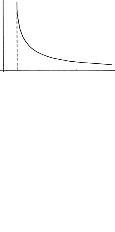
Figure 10.11 Plot of 2
max
for ions heavier than Si impinging onto Si. There
is less lateral spread for heavier ions, resulting in less damage. The same
basic trends occur for any substrate material, where ions heavier than the
substrate will form similar curves.
Focused ion beam systems278
10.7 Charging of the sample
Samples are not perfect conductors, and many samples have insulating
material on them which can accumulate excess charge on their surface as the
primary ion beam is scanned across them. This excess charge buildup is
generally positive, due to the positive ionic contribution from the primary
Table 10.2 Simulated damage depths layers in Si for various energies
of two different incident ions, Ga
þ
and In
þ
[8].
Ion energy
(keV)
Ga damage layer
(A)
In damage layer
(A)
Reduction
(%)
5785727
10 126 88 30
20 199 133 33
30 262 171 35
40 307 195 36
50 364 240 34
(a) (b)
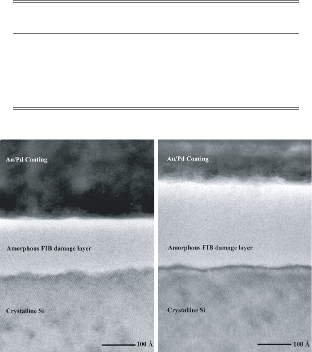
Figure 10.12 TEM micrographs from a study by Jami son [8] comparing the
damage layer thicknesses of different impinging ions. In (a) 30 keV In
þ
impinged on Si, while in (b) 30 keV Ga
þ
was used. These results agree with
the simulat ions in Figure 10.2, clearly showing the thickness of the damaged
crystalline structure is great er for Ga than In. The Au/Pd coating was added
as a preservation layer in making the TEM samples.
Micro-machining and mask repair 279
beam, and the release of negative charge from the sample by the secondary
electrons generated by the primary beam. In general, the primary beam
contributes about a third to a half of the total charge buildup. As the surface
of the sample acquires charge (positive), a voltage is built up on the sample
which can be as high as the primary beam voltage, resulting in unwanted
deflections of the primary beam and secondary electrons. In the worst case,
the primary ions normally impinging onto the sample can be entirely
deflected from the sample. Even in cases where the charging is not so severe,
the primary beam is deflected from its intended landing point, resulting in a
failure to cause the desired effects to happen where intended. Charging
manifests itself as complete or partial loss of imaging capability (the image can
completely disappear due to the secondary electrons being forced back to the
sample) or in the image jumping or showing regions of flaring brightness [3].
In the case of milling or deposition of material, charging makes that process
happen at the wrong position (primary beam deflection) or completely fails
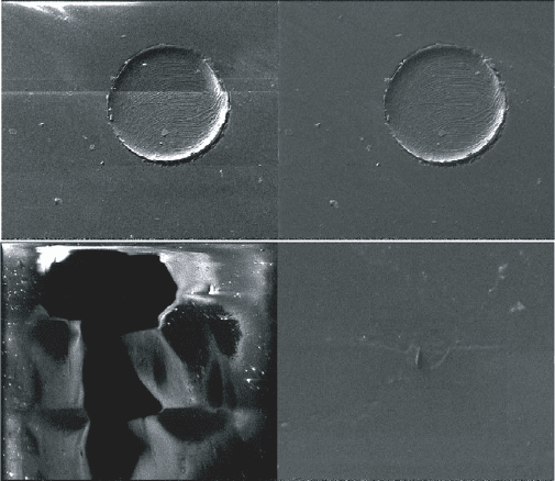
due to stopping the beam. Figure 10.13 shows examples of slight and con-
siderable charging on samples. In the first case (Figure 10.13(a)), the charging
(b)(a)
(d)(c)
Figure 10.13 The effects of charging on two different samples and the
neutralization of the effect. The top images are of an insulating membrane.
Image (a) shows the effect of mild charging, while (b) is of the same area but
with charge neutralization present. The bottom images are of plastic. Image
(c) shows considerable charging, whi le (d) was collected under the same
conditions, but with charge neutralization used.
Focused ion beam systems280
effect shows up as the bright area at the top left of the image, and the
horizontal line a third of the way down the image is where the primary beam
‘‘glitched’’ due to charge buildup. The lower micrograph (Figure 10.13(c))
shows how catastrophic the effect can be. There is complete loss of control of
where the primary beam impinges the sample, and the dark areas are where
the image information being collected from the secondary electrons is
extinguished due to the electrons being attracted back to the sample instead
of being collected by the imaging detector. In Figures 10.13(b) and (d) the
charge neutralization system has been employed to reduce the charging effect
to satisfactory levels.
There are several techniques to minimize or completely eliminate sample
charging. In some situations the sample can be pre-coated with a thin con-
ductive layer (C, Pt, or Au for example) giving the unwanted charge a path to
ground. While this can be used for some laboratory investigations, and some
failure analysis situations, it is not in general possible to radically so alter a
sample. In those cases where such a coating can be used, it is typically applied
with a thin film evaporator to a thickness of 0.1 nm, which if necessary can be
removed by RIE.
Another technique that works in many situations is to image a charging
sample by collecting secondary ions instead of secondary electrons. By pla-
cing a negative bias on the front of the detector, the secondary electrons from
the sample are returned to the sample surface, while positive secondary ions
are collected in the detector. Unfortunately, the secondary ion yields are
several orders of magnitude less than secondary electron yields for most
samples, so that reduced image quality may become a serious issue.
An adjunct technique used with secondary ion imaging, to reduce charging
effects, is to flood the surface with low energy electrons from an electron
source placed near the sample surface. By using low energy (10 –100 eV)
electrons to flood the sample surface, sites that are positively charged on the
sample attract the electrons until they are neutralized. The disadvantage of
this method is that secondary ion imaging must be used with the concomitant
loss of information for forming an image. One technique that can overcome
this situation is to multiplex the imaging detector and the electron gun
providing the neutralizing electrons. Typically, a control grid on the electron
gun is biased so as to provide electrons to the sample surface, while the
detector is biased not to collect electrons. The electron gun is then biased to
eliminate the electron current, the detector is enabled to collect electrons, the
primary ion beam is unblanked before scanning on the sample, and a line of
image data is collected. The primary ion beam is then blanked, and the
Micro-machining and mask repair 281
process is repeated. In a typical situation requiring charge neutralization, this
technique only adds about 1% to the total image collection time.
In some situations a useful charge neutralization technique is to introduce
water vapor onto the sample surface simultaneously while imaging or milling.
At the correct flux of water vapor, the excess surface charge can be bled
from the area undergoing modification or imaging. A user must introduce
water vapor with care, as some samples which contain hydrocarbons will
have their milling rate substantially increased selectively for the hydrocarbon
material.
10.8 Introduction of gases for deposition and milling enhancement
The use of auxiliary gases introduced into the sample chamber are covered
extensively in Chapter 4 of this volume. We point out here that the intro-
duction of gases can substantially and selectively increase the milling rate of
the sample [1, 2, 3]. This effectively reduces the work time and can be used in
many situations to differentially mill regions with a variety of materials
present. As pointed out in the previous section, the use of a gas can reduce or
eliminate the effects of charging.
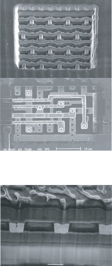
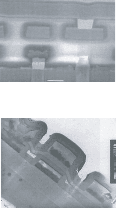
One example of gas assisted milling is shown in Figure 10.14, where this is
shown to emphasize the ability of the right gas to perform milling selectively.
Gases have been found that can selectively mill insulators rather than metals
(as shown in the figure) or that can selectively mill metals rather than insu-
lators. One might argue that the majority of future advancements in the use
of FIB will be centered around the development of ion beam–gas chemistry
interactions.
10.9 Milling artefacts
Due to the physics of the interaction of the milling beam with the sample,
there are artefacts that are caused by differential milling rates and geometric
effects. These artefacts initially were seen when making early attempts at
preparing sample cross sections, but can affect the work done while per-
forming a variety of other applications.
‘‘Waterfalls’’ (Figure 10.15) are the vertical stripes in the surface of a face
that has been exposed by milling adjacent material away. This effect arises
from surface topography and large differences in sputter rate for the mate-
rials present. This effect can be highly accentuated if gases are introduced
which are selective between the materials that are present.
Focused ion beam systems282
‘‘Ridges’’ (Figure 10.16) are the horizontal stripes that are caused by either
the primary beam drifting during a final ‘‘polishing’’ step or insufficient milling
time to clean the face. When large beam currents are used to reduce the
necessary time to remove material to expose a face, the beam ‘‘tails’’ do not
(a)
(b)
Figure 10.14 Two images showing the great selectivity of gas assisted
etching. Both regions were milled with Ga
þ
while XeF
2
was introduced.
Only the metal structures remain after the milling.
1 µm
Figure 10.15 ‘‘Waterfalls’’ (the vertical stri pes in the face) are caused by
topographic and differential sputter rates.
Micro-machining and mask repair 283
allow a sharply cut face to emerge from the mill. If it essential to view the
structure of the face, a low current (the beam ‘‘tails’’ are reduced) polishing
step must be used where the beam is run parallel along the face to effect the
polish. Beam drift, which removes the beam from the face, and insufficient
milling time are the culprits.
Small drops (Figure 10.17) sometimes form on the face of a cross section,
and are almost certainly Ga which has congregated via diffusion. The
material in the primary beam (Ga) has to end up somewhere, and in some
materials into which it has been implanted, the diffusion rate is sufficiently
large to allow the Ga to ‘‘pool’’ into droplets. Sometimes they can be sput-
tered away, and in some cases they can be removed chemically (via a dilute
solution of HCl and alcohol to promote wetting).
1 µm
Figure 10.16 ‘‘Ridges’’ are the hor izontal stripes on the surface of the face,
which are caused by beam drift or insufficient milling time.
Figure 10.17 The small black droplets in this TEM sample are probably Ga.
Focused ion beam systems284
10.10 Beam placement accuracy – metrology and milling
Often overlooked when considering the use of machining tools at the micro-
and nano-level is the ability to accurately place the FIB beam onto the
sample where the user wants it. A pristine ion beam placed incorrectly, in
many cases, is more unwanted than a beam of moderate profile accurately
placed. Milling in the wrong place can be a waste of time in a good case and a
total disaster in the worst case. Potential data can be irretrievably lost or a
microstructure can be destroyed. There are several contributions to the beam
placement error that must be understood and minimized in order to achieve
the necessary performance. These effects can be divided into two major
categories, one of which involves the engineering of the FIB system, while the
other involves the limits imposed by nature. Some potential contributions to
beam placement accuracy are as follows:
1. Engineering considerations that can be minimized:
scan magnification mis-calibration;
scan noise (AC electronic noise);
scan–sample stage mis-alignment;
sample stage mechanical jitter;
ion optics instability – ion source instability either electrical or mechanical;
2. Issues involving nature with hard limits:
low signal/noise images;
sample charging;
sample damage.
The uncorrelated contributions would have their effects added in quad-
rature. The effects which involve mis-calibration, electronic noise, and
mechanical vibratio n, can i n princip le be lower ed to levels acc ept able for
work at the nanometer s cale. Becaus etheionbeamischargedandsputters
material f rom the sample onto which it is scanned, the last th ree con-
tributions are physical limitations that nature places on the operation of the
system. The optimization of image acquisition for the purpose of metrology
causes an increase in sample char ging and damage. Likewise, the opt imi-
zation of reduced sample charging and damage, yields images with insuf-
ficient signa l/nois e t o b e able to perform the necessary metrology. In the
case of the r epai r of photo-litho gr aphic masks , the require ment s for beam
placement accurac y at pres ent are to be able to pla ce the be am to withi n
15–25 nm of the desired landing point depending on the mask type. With
good engi neering practices, this is ac hievabl e, but due to the damag e
Micro-machining and mask repair 285
imparted to the sample by the ion beam, requires the marriage of FIB with
SEM and AFM technologies.
10.11 Micro-machining applied to the repair of masks
Most modern microelectronics is produced using optical lithography, where
light is used to expose photosensitive resist coatings. Almost all the steps in
these complex production processes are preceeded by a lithography step
where, for example, contact metalization or implantation doping is defined.
This patterning is achieved by the use of photomasks, which selectively block
and transmit light to the resist, or through the introduction of an attenuated
phase shift or a strong phase shift, thus transferring the pattern contained in
the mask to the resist. As feature sizes in microelectronics have shrunk,
several different kinds of masks have been developed. In the past, the mask
structure was chrome-on-glass (COG), also known as a binary mask, where
the chrome was used as the blocking medium. These are generally produced
by electron beam lithography, followed by chrome etch, resist removal, and
subsequent inspection for defects. There has been considerable work done in
developing phase shift masks to extend the resolution, contrast, and depth of
focus of optical lithographic tools beyond what is achievable with binary
chrome masks. In addition, techniques to bring about the desired patterns
have been developed called optical proximity correction.
Once the mask has been made, defects must be located and cataloged.
Since a single printable defect on a mask can bring the yield for a semi-
conductor device to zero, the defects must be removed, and fall into two
broad classes: clear defects and opaque defects. Clear defects are where
absorber material has not been placed properly, leaving holes through which
the light can pass, and the repair consists of depositing opaque material to fill
in the hole. Opaque defects are where excess absorber material blocks the
transmission of light, and the repair consists of removing the excess material.
There is a third kind of defect in alternative phase shift masks where the
substrate material has the wrong thickness to cause the correct phase shift.
Because of their ability both to mill away material and to deposit new
material at the sub-micrometer level, FIBs are natural candidates for use in
the repair of defective masks. As feature sizes have shrunk, new variations of
masks are under development, which include phase shifting masks and the use
of optical proximity correction techniques. While FIB is a candidate to repair
the various types of masks, fundamental limitations of FIB technology may
force FIBs to be used in conjunction with other techniques such as electron
Focused ion beam systems286
beams (EB) and atomic force microscopy (AFM). The integration of an FIB
and SEM has been covered in detail in Chapter 5. All of the facets of FIB
technology capability and limitation potentially converge in the repair of
masks.
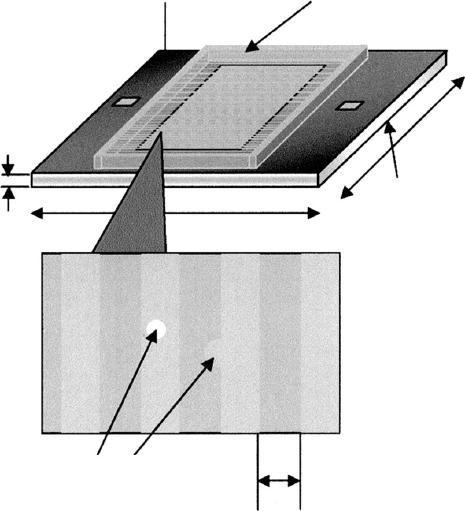
10.12 Mask structure
The basic structure of a photomask is shown in Figures 10.18 and 10.19. The
generic opaque and clear defects are shown, as well as cross sections of
generic types of masks [9,10]. The substrate of the mask, called the reticle,
contains the pattern to be transferred to the wafer, and is in general quartz or
some variation of quartz. The pellicle is a thin membrane or plate that is
placed between the mask and the projection optics in order to protect the
mask from contamination. Because pellicles can be made extremely thin and
uniform, when inserted into the optical path, they provide necessary pro-
tection, but do not introduce image degradation. The top cross section in
Pattern film
Pellicle
0.0064 m
0.1524 m
6 inches
Quartz substrate
Defect
CD
Figure 10.18 Generic mask structure showing a typical size and component
parts, as well as two types of defects.
Micro-machining and mask repair 287