Graef M. Introduction to conventional transmission electron microscopy
Подождите немного. Документ загружается.

178 The transmission electron microscope
3.6.2 Quadrupole elements
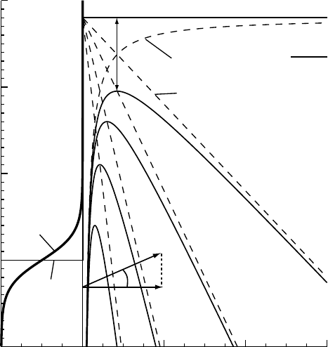
A quadrupole lens is a lens with two orthogonal planes of symmetry, and two
additional planes of anti-symmetry oriented at 45
◦
with respect to the symmetry
planes (Fig. 3.20a). In the absence of currents in the field region, the magnetic
induction inside such a lens can be derived from the scalar magnetic potential
ω(x, y, z). One can show [Szi88] that this potential is to a good approximation
described by
ω(x, y, z) = F(z)xy,
where F(z) is a function which describes the axial variation of the flux density.
Equipotential contours for this potential are shown in Fig.3.20(a). The magnetic
field components are determined from the gradient of the scalar potential:
B
x
=−µF(z)y
B
y
=−µF(z)x
B
z
=−µF
(z)xy.
Figure 3.20(b) shows such a magnetic field configuration in between the pole
pieces. Note that if F(z) is constant inside the quadrupole lens, then there is no
axial component to the field and the field components lie entirely in a plane per-
pendicular to the optical axis. For electrons traveling nearly parallel to the optical
axis the resulting Lorentz force will also be normal to the axis. Because of the cross
product nature of the Lorentz force we find that the force vectors are tangent to
the equipotential lines for an electron traveling parallel to the optical axis. Such a
field geometry may hence be used to change the shape of the electron beam. Con-
versely, a beam affected by astigmatism can be restored to a circular shape. The
main use of quadrupole lenses in the transmission electron microscope is therefore
to correct astigmatism in the beam. This is typically done at two locations: the first
set of quadrupole lenses is located between the last condensor lens and the beam
deflectors. A photograph of such a correction coil is shown in Fig. 3.20(c). This
correction coil is actually a pair of quadrupoles oriented at 45
◦
with respect to each
other. This permits adjustments of the beam shape in two orthogonal directions.
The second set of astigmatism correctors is located immediately below the objective
lens lower pole piece, and is typically much smaller than the condensor stigmator –
a photograph is shown in Fig. 3.20(d). These correction coils are among the most
important components of a modern electron microscope. We will see in Chapter
10 that without astigmatism correction coils, the resolution of a TEM would be
around 1 nm, not good enough for observations at the length scale of interatomic
distances.

3.7 Basic electron optics: electron guns 179
3.7 Basic electron optics: electron guns
3.7.1 Introduction
In this section, we will discuss one of the most essential components of a TEM: the
electron gun. The main purpose of the electron gun is to provide a steady stream
of electrons with a constant kinetic energy, i.e. a monochromatic electron beam.
Ideally, the electrons should appear to emanate from a single point on the filament
surface, so that the gun can be described as a point source. In addition, since we
have seen in the preceding sections that several lens aberrations depend on the
angle between the trajectory and the optical axis, the electrons should travel close
to the optical axis, at very small angles to the axis. Finally, after passing through
the entire column (including the sample) there must be sufficient electrons left over
to form an image on the detector (screen, micrograph, etc.) to acquire the data in
a reasonable amount of time (exposure time). This means that the image current
density, the number of electrons per second that hit a unit area of the detector, must
be reasonably high.
These qualitative statements can be cast into more precise mathematical terms,
and the design of electron guns is a highly specialized field, similar to the de-
sign of magnetic lens elements. The basic design process goes as follows: for a
given geometry of the filament and all potential surfaces around the tip, the elec-
tric equipotential surfaces are computed, typically by finite element analysis. The
trajectory equation is solved for a large number of trajectory starting points, and
the properties of the assembly are computed, including aberrations. The design
parameters are then varied until the desired functionality is obtained.
We will discuss the various types of electron guns in the following subsections.
First, we will describe the physics behind the process of electron emission.
3.7.2 Electron emission
In this section, we will closely follow a paper by Fransen et al. [FCRT
+
99] and
Chapter 44 in [HK89b]. For simplicity we will represent the surface of the filament
tip as a flat surface of unspecified lateral dimensions. The z-axis is taken to be normal
to the surface. At absolute zero, the energy distribution of the electrons inside the
metal is rather simple: all energy levels up to a maximum energy are occupied.
This maximum energy is known as the Fermi energy E
F
. When the temperature
is increased, some electrons will gain sufficient thermal energy to occupy higher
energy states. The distribution of occupied states is described by the Fermi–Dirac
distribution:
f
(
E, T
)
≡
1
1 + e
[
E−(E
F
−V
0
)
]
/k
B
T
, (3.46)
180 The transmission electron microscope
Energy (eV)
0
1
2
3
-1
10246
z (nm)f (E, T)
0 K
1800 K
W
image charge
applied field (W - eFz)
F=0.5 V/nm
F=1
F=2
F=4
∆W
(
W -
e
2
16πε
o
z
)
p
θ
p
z
Fig. 3.21. Schematic illustration of the Fermi–Dirac function at 0 and 1800 K (left-hand
side). The barrier potential V (z) (in eV) is shown as a solid line for applied field strengths
of F = 0.5, 1, 2, and 4 V nm
−1
, and a work function W = 2.8 eV. The components of V (z)
are shown as dashed lines. (This figure is based on Fig. 2 in [FCRT
+
99].)
where k
B
is the Boltzmann constant (8.618 16 × 10
−5
eV K
−1
), and V
0
is a constant
used to adjust the energy origin. As the temperature increases, the Fermi–Dirac func-
tion develops a high-energy tail, as shown on the left in Fig. 3.21 for a temperature
of T = 1800 K and V
0
= E
F
.
The energy needed for an electron to escape the metal is given by the work
function, W . The work function is equal to the difference between the vacuum
energy level and the Fermi level, and depends on both the atom type and the crystal
plane forming the metal surface. For pure tungsten the work function is 4.5 eV, while
for ZrO-coated (001) tungsten, W is reduced to 2.8 eV. If the filament temperature
is sufficiently high so that energy states above the vacuum level are occupied,
then electrons will be emitted into the vacuum. This process is known as thermal
emission. If an electric field is applied between the metal surface and an external
electrode, then the vacuum level becomes a function of the distance to the surface
and is represented by the barrier potential V (z). It is customary in the electron
emission literature to represent this electric field by the symbol F instead of E,
since E is already taken to represent the microscope acceleration voltage.

3.7 Basic electron optics: electron guns 181
The energy V (z) depends on the workfunction W , the applied field F, and also
on the Coulomb interaction between the emitted electron and its mirror image in
the metal surface. An explicit expression is given by
V (z) = W − eFz −
e
2
16π
0
z
(z > 0); (3.47)
= W − Fz −
0.359 95
z
[
eV
]
(with F in V nm
−1
, z in nm).
The zero of potential energy in this case is taken at the Fermi level. Figure 3.21
shows the function V (z) for several field strengths F and a work function of 2.8eV
[FCRT
+
99]. The dashed lines indicate the Coulomb term and the electric field term.
It is clear that with increased applied field strength the barrier energy becomes lower
by an amount W . This lowering is known as the Schottky effect. It is left to the
reader to show that
W =
/
e
3
F
4π
0
= 1.1998
√
F
[
eV
]
(with F in V nm
−1
). (3.48)
The main question to be answered is then: what is the emitted current density
in the z-direction at a given temperature and applied field? While the general solu-
tion to this problem is still unknown, there are several special cases for which an
approximate analytical solution is possible. For an electron that has left the metal
with momentum p we have a total energy of
E =
p · p
2m
+ V (z).
This energy can be decomposed into components normal and tangential to the
surface. We define (following [HK89a])
U
n
≡
1
2m
p
2
z
+ V (z); U
t
≡
1
2m
p
2
x
+ p
2
y
.
Not every electron with the correct energy will actually escape from the metal. A
fraction of the electrons will be reflected from the surface and return to the bulk of
the metal. The fraction of electrons that is actually emitted is described by D(U
n
),
the transmission coefficient.
Next, we consider an elementary volume in momentum space, d
3
p.Ifweuse
cylindrical coordinates, as shown in Fig. 3.21, then we can rewrite this volume

182 The transmission electron microscope
element as
d
3
p = sin θ p
2
dp dθ dφ,
= sin θ p( p d p)dθ dφ,
= sin θ
2m(E − V (z))(m dE)dθ dφ,
where we have used p
2
= 2m[E − V (z)] and p dp =
1
2
d(p
2
) = m d( p
2
/2m) =
m dE. The total number N (p) of electrons with momentum between p and p + dp
that have enough energy to escape the metal is given by the product of the number of
quantum states per elementary volume in momentum space (2/ h
3
), the probability
that the electron will have the correct energy (the Fermi–Dirac function), and the
probability that the electron will not be reflected (D(U
n
)), or
N (p) =
2
h
3
D(U
n
)
1 + e
(E −E
F
)/k
B
T
.
The current density element d
3
j is then given by
d
3
j = e
p
m
N (p)d
3
p
=
2e
mh
3
p f (E, T )D(U
n
)d
3
p. (3.49)
Since we are mostly interested in the current density component along the
z-direction we can use p
z
=
√
2m[E − V (z)] cos θ to obtain [FCRT
+
99]:
d
3
j
z
=
2me
h
3
[E − V (z)]
1 + e
(E −E
F
)/k
B
T
D(U
n
) sin 2θ dE dθ dφ. (3.50)
For a given model for D(U
n
) and V (z), this equation can be integrated over all
angles (0 <φ<2π ;0<θ <π/2), and over all appropriate energies to obtain the
total emitted current density. We will now consider some special cases for which
these integrations can be carried out analytically.
3.7.2.1 Thermionic emission
In the case of thermionic emission, there is no external applied field and the origin
of the energy scale can conveniently be chosen to coincide with the vacuum level.
The potential barrier in the absence of a field vanishes outside the crystal, and
the transmission coefficient D(U
n
) = 1 for positive U
n
. At high temperature, the
Fermi–Dirac function can be simplified by dropping the 1 in the denominator and

3.7 Basic electron optics: electron guns 183
we find for the current density (3.50):
j
z
=
2me
h
3
.
2π
0
dφ
.
π/2
0
sin 2θ dθ
.
+∞
0
Ee
−(E +W )/k
B
T
dE,
= AT
2
e
−W/k
B
T
≡ j
T
, (3.51)
with
A =
4πmek
2
B
h
3
= 1.201 75 × 10
6
A
m
2
K
2
.
This equation is known as the Richardson–Dushman equation, and can be used to
determine the work function W from measurements of the current density j
z
(T )
at different temperatures. For a tungsten filament with W = 4.5 eV, operated at
T = 2700 K, we have j
T
≈ 3.5Acm
−2
. A lanthanum-hexaboride filament (LaB
6
)
with a work function of W = 2.7 eV is typically operated between T = 1800 K
( j
T
= 10.7Acm
−2
) and T = 1900 K ( j
T
= 29.9Acm
−2
).
3.7.2.2 Schottky emission
We have seen previously that in the presence of an electric field F of the order of
1Vnm
−1
the barrier energy is reduced by an amount W . The emission current
density of a Schottky emitter is then given by equation (3.51) with W replaced by
W − W ,or
j
S
= e
W/k
B
T
j
T
. (3.52)
The emission current is hence enhanced with respect to the thermionic emission
current. For a ZrO-coated tungsten single crystal filament with a work function of
W = 2.8 eV and an applied field of 1 V nm
−1
(W = 1.2 eV), the current density is
j
S
= 1.3 × 10
4
Acm
−2
, about three orders of magnitude larger than for thermionic
emission.
Equation (3.52) is valid as long as tunneling through the potential barrier can
be ignored. If the applied field is sufficiently strong, so that the potential barrier
becomes narrow (Fig. 3.21), then the transmission coefficient D(U
n
) must be com-
puted explicitly. This is beyond the scope of this textbook and we refer to [FCRT
+
99]
for an explicit derivation of the so-called extended Schottky emission.
3.7.2.3 Thermal field emission
In thermal field emission the temperature of the filament is kept low (room tem-
perature) so that the high-energy tail of the Fermi–Dirac function nearly vanishes.
Electrons can only escape from near the Fermi level by tunneling through the nar-
row potential barrier, as shown in Fig. 3.21 for F = 4Vnm
−1
. The applied field
184 The transmission electron microscope
is typically several volts per nanometer and the current density computation be-
comes rather lengthy; we refer to Fransen et al. [FCRT
+
99] for a brief description
and Kasper [Kas82] for a detailed account. The current density for thermal field
emission is given by
j
TF
=
4πme
h
3
d
2
e
−bW/d
π p
sin π p
. (3.53)
The factor d is a function of the applied field and the work function (see [Kas82]):
d =
ehF
4πt(W/W )
√
2mW
=
9.7598 × 10
−2
t(W/W )
F
√
W
[eV] (F inVnm
−1
, W in eV),
with
t(y) = 1 + 0.1107y
1.33
,
b ≈ 0.6, and p = k
B
T/d. Equation (3.53) at T = 0 K is known as the Fowler–
Nordheim equation. For non-zero temperatures the equation is only accurate for
p < 0.7. Comparison with the Richardson–Dushman equation shows that d takes
on the role of k
B
T . For a tungsten field emission tip operated at room temperature
(T = 300 K) and an applied field of 7 V nm
−1
,wehaved = 0.3eV, p = 0.085,
and j
TF
= 1.9 × 10
5
Acm
−2
.
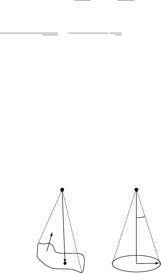
3.7.2.4 Beam brightness
Let us assume that all electrons emanate from a circular region of radius r on the
tip of a filament. An observer at P, a distance q from the filament (Fig. 3.22b), will
then “see” an electron source with a surface area of πr
2
. The size of this source is
typically expressed as a solid angle rather than a surface area, since the apparent
P
S
n
r
P
r
q
θ
(a) (b)
Fig. 3.22. Definition of the solid angle and the aperture semi-angle θ; (a) general case and
(b) for a cone.

3.7 Basic electron optics: electron guns 185
surface area depends on the distance q. Solid angle is defined as the area subtended
by a surface S when looking at that surface from a reference point, divided by the
square of the distance to that surface,or
(S) =
..
S
r · n
r
3
dS
with n the outward normal to the surface (Fig. 3.22a). For a sphere, the solid angle,
when looking from the center of the sphere, is equal to
=
.
π
0
.
2π
0
sin θ dθ dφ = 4π.
The unit of solid angle is the steradian. The solid angle subtended by the base of a
cone with base radius r when viewed from the top is
=
πr
2
q
2
= πθ
2
(see Fig. 3.22b) with q = r/θ the height of the cone.
The total current density j passing through the point P is proportional to the
solid angle subtended by the source at the point P, and the proportionality factor
β is known as the beam brightness:
β =
j
πθ
2
. (3.54)
Brightness is measured in amperes per unit area per steradian. If we represent the
current density j by the current I divided by the area A, then we can determine
how a magnetic lens affects the beam brightness. A magnetic lens with lateral
magnification M reduces the current density I /A to I /M
2
A
2
; the angular aperture
θ is increased by the angular magnification M
α
by a factor M
2
α
= 1/M
2
, so that the
total brightness remains unchanged. Brightness is hence a property of an electron
beam and is left unchanged by (aberration-free) magnetic lenses.
From the definition of brightness we find that a higher current density will in-
crease the brightness; in other words, if we can get more electrons to emanate
from the filament emission area with a momentum inside the cone centered at P,
then the current density and hence the brightness would increase. In Section 3.7.2
we have seen that the energy of the emitted electron could be separated into two
components U
n
(corresponding to the momentum p
z
and the barrier potential) and
U
t
(corresponding to the momentum components p
x
and p
y
). It is then easy to
see that a rapid decrease of current density with increasing tangential momentum
components (and therefore with U
t
) will produce a higher brightness. The (axial)

186 The transmission electron microscope
brightness can hence be defined as [FCRT
+
99, SM84]:
β ≡
e
ˆ
π
d j
z
dU
t
U
t
=0
, (3.55)
with
ˆ
the relativistic acceleration potential introduced in Chapter 2. We can com-
pute the brightness for the various emission mechanisms discussed in the previous
section. The resulting brightnesses are given by
β
T
=
e
ˆ
j
T
πk
B
T
(thermionic emission); (3.56)
β
S
=
e
ˆ
j
S
πk
B
T
(Schottky emission); (3.57)
β
TF
=
e
ˆ
j
TF
πd
(thermal field emission). (3.58)
The ION routine
emission.pro on the w
ebsite
can be used to display the barrier
potential V (z) and various quantities (current density, brightness, work function
reduction, etc.) for all three emission mechanisms described in this section. The
drawings produced by this routine are similar to that shown in Fig. 3.21.
Using the gun brightness we can compute the current density at any point along
the optical axis of the microscope, using equation (3.54). The current density in the
illumination spot after an aperture of diameter r, at a distance D from the aperture
plane, is given by
j
0
= πβ
)
r
D
*
2
.
For a tungsten hair-pin filament with β = 5 × 10
5
Acm
−2
sr
−1
[Spe88] the current
density for a 400
µm diameter condensor aperture (r = 0.2 mm) is then approxi-
mately 1 A cm
−2
, using an approximate value for D = 250 mm, measured directly
on the cross-section of the microscope column discussed earlier in this chapter. If a
smaller condensor aperture is used, the current density goes down but the brightness
remains constant. The image current density at the phosphor screen for a magnifica-
tion of M = 500 000 is then 4 × 10
−12
Acm
−2
, i.e. current densities at the viewing
screen are of the order of a few pA cm
−2
. This determines the exposure time for
electron micrographs, when it is combined with the sensitivity of the emulsion (see
Section 3.11 on electron detectors). The maximum brightness for a given electron
gun is proportional to the acceleration potential and increases exponentially with
temperature; the lifetime of a filament decreases with increased temperature, so
there is an optimum operating temperature for the filament.

3.7 Basic electron optics: electron guns 187
Table 3.2. Approximate parameters for different electron guns
(sources: [Spe88, Rei93, WC96, FCRT
+
99]).
Thermionic emission Field emission
Tungsten LaB
6
Schottky Field emission
Work function [eV] 4.5 2.7 2.8 4.5
Operating temperature [K] 2700 1700 1800 300
Current density [A cm
−2
] 1–3 25–100 10
4
–10
6
10
4
–10
6
Virtual source diameter [nm] 50 000 10 000 10–15 3–5
Brightness [A cm
−2
sr
−1
]10
4
10
6
10
8
–10
9
10
8
–10
9
Energy spread [eV] 1–3 0.5–2 0.3–1.0 0.2–0.3
Required gun vacuum [Pa] 10
−3
10
−5
10
−7
10
−8
Lifetime [h] 25–100 500–1000 >1000 >1000
Cost [U.S.$] 10–100 400–1200 1500–3500
a
1500–3500
a
Does not include installation costs.
3.7.3 Electron guns
In the previous section, we have described how many electrons are emitted from the
filament tip for a given work function, temperature, and applied field. The shape of
the filament tip and the geometry of the applied field did not enter the discussion at
any point. In reality, the geometry becomes very important because it determines
the trajectory of the electron once it has been emitted from the tip. Solving the
trajectory equations for a given gun geometry is far beyond the scope of this book
and we refer the interested reader to Chapters 43–50 in [HK89b] and references
therein.
In this section, we will describe the structure of the electron gun. Several differ-
ent gun types are available based on thermionic emission, (cold) field emission, or
Schottky field emission. Table 3.2 shows some of the relevant parameters for the
different electron guns. Descriptions of measurement techniques for gun charac-
teristics can be found in [Spe88, Section 7.2] and [WC96, Section 5.5].
3.7.3.1 Thermionic electron guns
Figure 3.23(a) shows a schematic drawing of the components of a thermionic
electron gun, also known as a triode gun, along with a photograph of the cross-
section of the gun of a JEOL 120CX TEM (Fig. 3.23b). The gun consists of three
basic components: the filament (F), the grid or Wehnelt cap, and the anode. The
filament is typically a hairpin-shaped tungsten wire or a pointed tungsten wire. In
the latter case the pointed wire is spot-welded to a tungsten support wire. A voltage
V produces a resistive heating current I
F
through the filament wire. Tungsten