Yao N. Focused Ion Beam Systems: Basics and Applications
Подождите немного. Документ загружается.

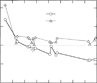
angle dependence as backscattered ions, because the recoil cascade approa-
ches the surface as the incidence is inclined. Figure 4.11 shows the fitting
parameter f as a function of the atomic number, Z
2
, of materials under 10 keV
electron impact and 30 keV Ga ion impact, where the fit is applied to the
calculated results for the angles of less than 60
o
[60]. For electron impact, the
backscattering effect changes the f value from above 1 to below 1 as
the backscattering coefficient increases with increasing Z
2
. On the other hand,
due to the small contribution of the backscattered ions and the recoiled target
atoms to kinetic emission, the general dependence approximately obeys the
inverse cosine law ( f ¼1), except for low-Z
2
materials ( f > 1) where the
contribution of recoiled target atoms largely increases.
Further study of topographic contrast is required to resolve differences in
topographic contrast of SE imaging in the FIB and SEM systems. The
topographic contrast is convolved with detector geometry and configuration
to produce an image with many features familiar to the casual observer. It
should be noted that topographic contrast is frequently overwhelmed by
channeling contrast in certain material systems and geometries, pointed out
by Prewett and Mair [64].
4.3.3 Channeling contrast
Channeling (orientation or grain) contrast is perhaps the most striking fea-
ture of FIB microscopy of metallic samples, and arises from channeling of the
0
10
20
30 40
50
60
70
80
Target atomic number, Z
2
2.0
1.5
1.0
0.5
0
10 keV e
30 keV Ga
Fitting parameter, f
Figure 4.11 Calculated fitting parameter f in ()/(0) ¼(cos )
f
and
–()/–(0) ¼(cos )
f
as a function of Z
2
for 30 keV Ga ion impact and
10 keV electron impact, respectively [60].
Focused ion beam systems108
incident ions between lattice planes of the sample. Depth of penetration of
the channeled incident ion varies with the relative angle between the ion beam
and the lattice plane and the interplanar spacing of the lattice. A typical SIM
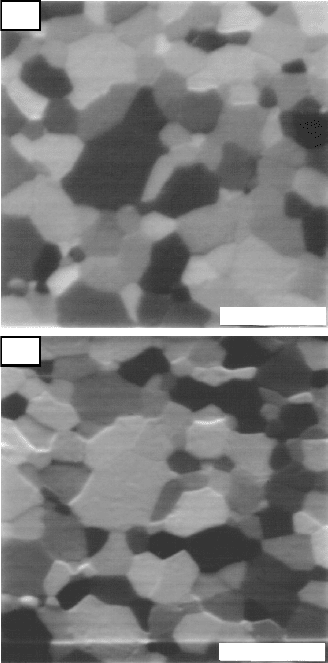
image showing the channeling contrast from the aluminum (Al) surface on a
silicon (Si) specimen is shown in Figure 4.12. The dark grains with low SE
yield correspond to the channeled grains.
Through channeling contrast of the SEM images, grains in polycrystalline
samples are seen with BSE (backscattered electron) contrast of the SEM
images that depends sensitively on the sample tilt [15]. This sensitivity results
from the dependence of the BSE yield on the orientation of the primary beam
relative to the lattice planes and is caused by the primary Bloch wave field.
1
2
(a)
1
2
(b)
5 mm
5 mm
Figure 4.12 Channeling contrast SIM images of Al layer on Si substrate. (a)
Image observed at an incident angle of fi ¼15
and (b) observed at fi ¼30
after a few minutes bombardment at fi ¼15
. Note: the bright grains in (a)
are more etched than the dark ones.
Imaging using electrons and ion beams 109
Due to the sensitivity of the variation on the surface, the channeling contrast
can decrease with an increasing electron-probe focusing angle which should
not exceed 1–10 mrad. The depth of average channeling varies with Z
2
, but
for most elements, the additional contribution to the contrast is much smaller
from depths > 50 nm. The channeling contrast is also very sensitive, either on
an amorphous surface oxide layer or multiple scattering in the crystal.
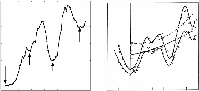
As to the directional effects of kinetic emission, experimental and theore-
tical work has been reviewed by Brusilovsky [65 ]. Fast particles entering
crystalline materials in low-index lattice directions are steered into the
interior of the target by many small-angle scattering collisions. This causes a
drastic reduction in the SE yield for two reasons: first, kinetic emission
depends on inelastic energy loss and channeled ion transfers relatively small
energy in each collision along its path; second, SEs generated deep in the
material have difficulty in escaping to the surface. Very recently, an experi-
ment [66] revealed that the fine changes in SE intensities in SIM with the tilt
angle was in reasonable agreement with the incident angle dependence of the
SE yield observed using an argon ion beam by Mashkova et al.[67] (Figures
4.13(a) and (b)).
According to the continuum model of Lindhard [68], the critical angle for
ion channeling is approximately estimated to be
9
c
/ðZ
1
Z
2
E
0
Þ
1=2
: ð4:12Þ
(a)
(b)
–20 –10 0 10 20 30 40 50 60
0.4
0.8
1.6
2
2.4
2.8
3.2
4
3.6
1
2
3
4
0
20
40
60
Tilt an
g
le (de
g
rees)
Relative intensity
2
1
0˚
(001)
20˚
(114)
36˚
(112)
54˚
(111)
y
Figure 4.13 (a) Relative SE intensity for the FIB-SIM as a function of the
Ga ion beam angle tilted on a Cu crystalline surface [66]. (b) Incident angle
dependence of SE yield of a Cu crystalline due to the impacts of Ar ions
with the energies of 30 keV (1) and 20 keV (2) [67]. (Adapted from [66].)
Focused ion beam systems110
The experimental 9
c
values mostly range from 5 to about 20
o
, which
are sufficiently larger than the FIB focusing angles of a few mrad. A clear
contrast, as shown in Figure 4.12, has been obtained after removing the
native oxide surface layer with a high SE yield. On SIM imaging, channeling
contrast has been mostly observed for metals such as Al, Cu, Fe, Ni, and Au,
but not for semiconductors of Si, GaAs, etc. At first sight one might expect
severe disruption of the crystalline caused by the ion beam to amorphize the
surface. A plausible explanation by R. Shimizu (Osaka Institute of Tech-
nology, Pers. Comm.) is that many metals remain crystalline as a result of
fast recrystallization under ion bombardment at room temperature.
4.3.4 Spatial resolution and information depth
The SEs have information along their own trajectories in addition to the
trajectories of the projectiles that excite the SEs of interest. Most of the SEs
are produced in the surface layer, as they are independent of the incident
probe. Under electron impacts, the SEs consist of two components which
correspond to the SEs excited by PEs (primary electrons) and BSEs (back-
scattered electrons), respectively. The SEs excited by PEs have a small spatial
spread of < 10 nm, but the SEs excited by BSEs have a large one of several
tens to several hundreds of nanometers, decreasing PE energy. Under the Ga
ion impacts, the spatial spread of SE information is roughly as small as
10 nm, decreasing with an increasing Z
2
.
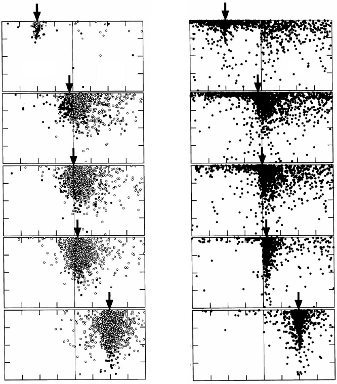
Figures 4.14(a) and (b) show birthplaces of the SEs that have escaped from
the surface at various beam incident positions near the Al–Au boundary
[4 ,55]. Incident probes for SIM and SEM imaging are assumed to be the
point beams of 30 keV Ga ions and 10 keV electrons, respectively. The SEs
for the Ga ion impact are classified into three types because of the collision
partners: projectile ion (black), recoiled target atom (white), and cascade
electron (gray). It can be observed that the three components contribute
equally to the SE yield for the low-Z
2
sample (Al). For the high- Z
2
sample
(Au), however, the electron excitation by the projectile ions dominates those
by both the recoiled target atom and the cascade electrons. A large number of
SE birthplaces for both ion and electron impacts are < 5 nm in depth. For the
ion impacts, a laterally narrow spread of the SE birthplace shown in Figure
4.14(a) is caused by the short ranges of the projectile ions, recoiled target
atoms, and cascade electrons. Under electron impacts, on the other hand, the
SEs excited by PEs have a small lateral spread of < 10 nm, but the SEs
excited by BSEs have a large one of several hundreds of nm, as mentioned
above [34].
Imaging using electrons and ion beams 111
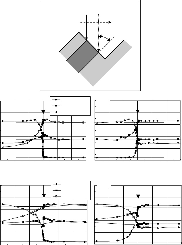
Assuming the SIM and SEM observations of an FIB milled cross section,
we consider a layered sample to have an Al–Au–Al structure, the cross sec-
tion of which is tilted by /4 radians with regard to their probe incident
directions, as shown in an inset in Figure 4.15 [4]. All the yields of SEs for
0
5
10
15
Depth (nm)
0
5
10
15
Depth (nm)
0
5
10
15
Depth (nm)
0
5
10
15
Depth (nm)
0
5
10
15
Depth (nm)
0
5
10
15
Depth (nm)
0
5
10
15
Depth (nm)
0
5
10
15
Depth (nm)
0
5
10
15
Depth (nm)
0
5
10
15
Depth (nm)
20
15
10
5
0
5
10
15
20
Lateral (nm)
20
15
10
5
0
5
10
15
20
Lateral (nm)
(a)
(b)
Au
Au
Al
Al
Figure 4.14 Birthplaces of SEs that have escaped from the surface (made of
Au and Al by halves) due to the beam impacts of (a) 30 keV Ga ions and (b)
10 keV electrons [4,55]. The arrows indicate the impact points on the surface.
The number of projectiles is 10
4
. In (a), the SEs are excited by projectile ion
(black), recoiled target atom (white), and cascade electron (gray).
Focused ion beam systems112
Au
Al
Al
P
1
P
2
Au
Al
Al
P
1
P
2
Au
Al
Al
P
1
P
2
Au
π/4
Scan
30 keV Ga ions or 10 keV electrons
0.8
1
–30 –20 –10 0 10 20 30
Au Al
(b2)
P
2
0
0.2
0.4
0.6
0.8
1
–30 –20 –10 0 10 20 30
Beam
p
osition (nm)
Al Au
(b1)
P
1
1
–150 –100 –50 0 50 100 150
Beam position (nm)
Au Al
(a2)
P
2
0
0.2
0.4
0.6
0.8
1
–150 –100 –50 0 50 100 150
Beam position (nm)
Al Au
(a1)
P
1
γ (30 keV Ga)
δ (10 keV e)
η (10 keV e)
γ (30 keV Ga)
δ (10 keV e)
η (10 keV e)
, and
Figure 4.15 Line profiles of SE yield for 30 keV Ga ions and SE yield – and
BSE yield · for 10 keV electrons as a function of the beam scanning position
for /4-tilted sample revealing a cross-sectional Al-Au-Al structure [4]; (a1)
near the boundary (P
1
) between Al and Au and (a2) near the boundary (P
2
)
between Au and Al; (b1) and (b2) magnified profiles at the boundaries P
1
and P
2
corresponding to the profiles of (a1) and (a2), respectively.
Imaging using electrons and ion beams 113
30 keV Ga ion impact, and SEs and BSEs for 10 keV electron impact are
plotted as a function of the ion or electron scanning position in Figure 4.15.
The profile sharply changes at both the boundaries of Al–Au (P
1
) and
Au–Al (P
2
) and is roughly symmetric between the boundaries due to the
substructure effects. It is predicted that SEM images using the SE and BSE
signals show a combination of an indistinct or dull change of the image
brightness at the Al–Au boundary (P
1
) with a distinct or sharp change at the
Au–Al boundary (P
2
). Another interesting point is that the beam positions
corresponding to the half contrast of the line profiles at the boundaries are
shifted from the exact points of P
1
and P
2
. Therefore, SIM imaging is better
in spatial resolution for the structure/material measurements than SEM
imaging. Decreasing the electron impact energy is a direct method for
reducing the depth profiles of SEs.
4.3.5 Relevant subjects
This section discusses the relevant subjects on the SIM imaging, i.e., charging
up for insulator samples and image deterioration due to sputtering.
Charging up
For insulator samples (including electrically floated conductors), charge will
build up on the surfaces while the primary ion beam (i.e., Ga
þ
FIB) is being
scanned across them. The charging up causes unwanted deflections of the
primary beam as well as SEs emitted from the sample. The former deflection
reduces the positional accuracy of the SIM imaging and FIB milling. The
latter deflection makes the SE detection yield fluctuate with the ion bom-
barding time and/or the bombarding position. Then, the image intensity is
locally or wholly modulated to become too dark or too bright. There are two
ways of solving this problem: (i) coat the samples with a conductor (e.g., Au,
Pt, C), or (ii) an electron beam flood to compensate for the positive charging
up. The other method is ultra-violet (UV) irradiation, where the light pene-
tration induces a conductive modulation in the semiconductor surfaces.
Coating is usually done using a thin film coater (or evaporator). As a
variation of the external coating, an FIB assisted deposition (FIB-AD) of
conductor films is used to do the selective coating and to connect the char-
ging site to a known ground site. In the case of the use of electron flooding of
low energies to neutralize the incident positive charge on the sample, SEs are
no longer used as the SIM imaging signal because no discrimination can be
made between the SEs and the flood electrons. Positive secondary ions (SIs)
Focused ion beam systems114
are now used instead of the SEs, but the SI intensity is rather smaller than the
SE one to deteriorate the SIM image quality. In the FIB cross-sectioning of
nonconductive materials, for example, the rough milling using a high-current
FIB of up to 30 nA requires the built-up charge to be dissipated using the
methods mentioned above. In the final milling using a low-current FIB of less
than 100 pA, on the other hand, little charging up is observed if the milled
surface connects to somewhere at ground level. The reason is that the
implanted Ga atoms make the surface conductive. Even a high-resistivity
surface is generous with the scanning beam of low current.
In the SEM imaging for the insulator samples, on the other hand, the
primary electron energy is popularly adjusted to some specified energy in the
range of 200 eV to 2 keV (depending on the sample) so as to balance the SE
yield. This method is not applied to the SIM imaging using the positive ion
probe. The SE emission does not decrease the positive charges building up on
the surface, but does increase them.
Deterioration in the SIM image quality due to sputtering
To form a good image, there must be resolution, contrast, and adequate
signal-to-noise ratio (S/N). Good images are essentially a system issue, i.e.,
the instrument plus sample. Unnecessary ion bombardment must be reduced
to minimize the unavoidable influence of ion sputtering and redeposition of
sputtered atoms.
In order to obtain an image of a given S/N, the beam must dwell at points
on the sample for a time t
d
to collect enough SE quanta. The number of
detected SE quanta per pixel is given by
N
e
¼ I
b
t
d
·=e; ð4:13Þ
where is the SE yield, · is the detection efficiency of SEs (taken to be 1 to
simplify the model), and e is the electron charge. The average human eye
requires an S/N value of at least 5. Considering a two-step process where by
primary ions strike a sample and generate SEs under Poisson statistics, the
number of incident ions per pixel N
ion
forms the image at S/N given by [6,10]
ðS=NÞ¼f=ð1 þ Þg
1=2
N
ion
1=2
: ð4:14Þ
Assuming · ¼1 and ¼2, the image at S/N ¼10 requires N
ion
¼150, i.e.,
t
d
¼24 msatI
b
¼1 pA, or an image acquisition time of 6.3 s for a 512 · 512
pixel image, and subjects the surface to erosion by 150Y atoms. Here, Y is the
sputtering yield, i.e., about 1–10 for 30 keV Ga ion bombardment, depending
on the target.
Imaging using electrons and ion beams 115
Looking closer at the sputtering spot, it can be seen that a scanning FIB
forms a local slope on the bombarding spot due to the difference in ion dose
between the beam head and tail positions in the scanning direction [69]. The
slope angle strongly varies with the scanning speed, the beam density, the
beam size, sputtering yield, and redeposition. Since a change in the slope
angle corresponds to that in the beam incident angle, the beam scanning
conditions also influence the parameters and Y. In high-resolution SIM
imaging, a single slow scan is usually superior to averaging frames to enhance
the S/N ratio of the image.
In SEM imaging, we don’t usually need to care about the sputtering, but it
does meet a contamination problem. Hydrocarbon molecules on the sample
surface are cracked and polymerized by the knock-on and/or ionization
processes. A carbon-rich contamination film grows over the electron scan-
ning area. At a thickness of the order of 10 nm, the SE emission will be of
carbon and the irradiated areas will appear darker in the SEM image.
4.4 Some applications of FIB linked with modern SEM/STEM/TEM
4.4.1 FIB micro-sampling and micro-fabrication
In FIB applications of micro-machining and device transplantation, FIB
sputtering plays the role of ‘‘cutter’’ and FIB induced deposition does the role
of ‘‘attacher’’ [ 70]. One of their successful uses is an FIB micro(m)-sampling for
site-specific SEM/STEM/TEM inspection. The micro-samples are dug out
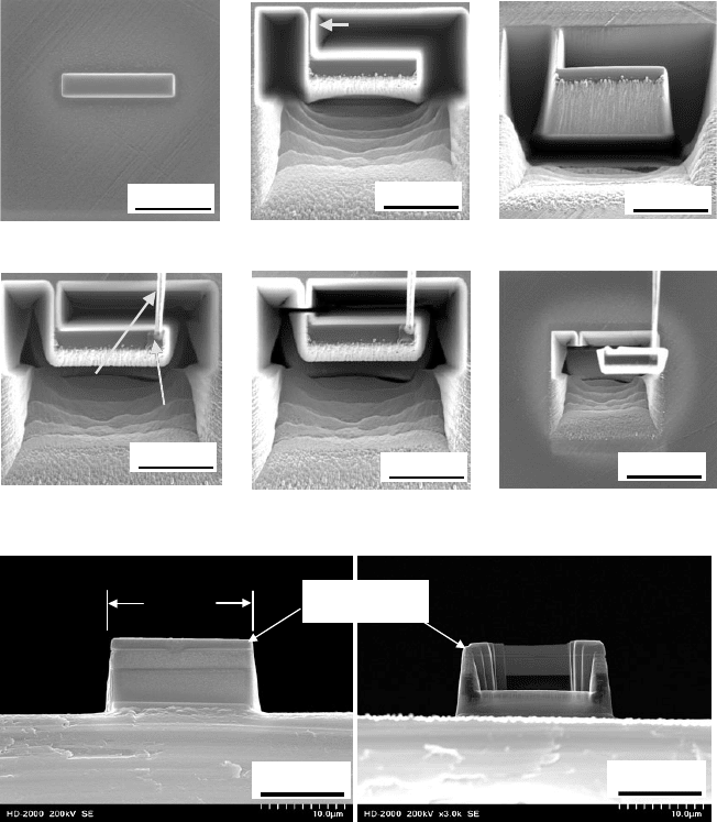
by FIB milling without cleaving a wafer or a chip [71,72]. Figure 4.16 shows a
schematic flow of the m-sampling for transmission electron microscope
(TEM) / scanning TEM (STEM) inspection. First, the m-sample (or m-wedge)
of interest (typically 3 mm wide · 13 mm long · 7 mm deep) is FIB dug-out,
leaving a micro-bridge (or a microbeam) to support the m-sample. Second, a
built-in metal needle (or m-probe) is manipulated into position for lifting the
m-sample. FIB assist-deposition (FIB-AD) is used to bond (or weld) the
needle to the m-sample. Further FIB milling of the micro-bridge separates the
m-sample from the wafer or chip. The separated m-sample is transferred and
then fixed onto the side of a partially cut TEM-grid using FIB-AD. Finally,
the m-sample is FIB thinned to a strip of about 0.1 mm thick and 7 mm long
and is ready for the TEM/STEM inspection. All the steps are accomplished
under vacuum in the FIB system. SIM images allow monitoring of each step
in live time thereby assisting the operator. Advantages of the FIB m-sampling
for TEM/STEM are as follows: (i) the wafer is left intact, (ii) FIB rethinning
is possible after TEM/STEM observation, (iii) it is possible to prepare the
Focused ion beam systems116
(a)
(d)
(e)
(f)
(b) (c)
(
g
) (h)
µ-bridge
probe
W-deposition
10 mm
10 mm
15 mm
10 mm
10 mm
10 mm
20 mm
10 mm
10 mm
m-sample
Figure 4.16 Schematic flow of the m-sampling for TEM/STEM inspection.
(a) Tungsten (W) deposition as a pro tection layer on the site-specific region
of interest, (b) FIB trench-milling to dig out the m-sample, leaving a m-bridge
(or a microbeam) to support the m-sample, (c) FIB cutting the m-sample
bottom, (d) bonding the m-sample to the m-probe, (e) FIB cutting the
m-bridge to release the m-sample from the wafer or chip, and (f) lifting the
m-sample to transfer onto TEM grid. All pictures in (a)–(f) are SIM images
to assist the operator. Pictures of (g) and (h) show 200 kV SEM images of
the m-sample attached on the TEM half-grid edge before and after the FIB
rethinning, respectively.
Imaging using electrons and ion beams 117