Yao N. Focused Ion Beam Systems: Basics and Applications
Подождите немного. Документ загружается.

effectively accomplishing the milling. The graph shows the corresponding SE
signal. As suggested in the graph, the FIB scanning is usually slower than the
SEM although this is not a strict necessity. The signal that forms the image is
the total SE signal, or the sum of both graphs in Figure 5.8. Two effects can
be observed in ‘‘live’’ SE images: first, an offset in brightness compared to
SEM-only images (because of the DC part of the FIB generated SE signal);
and second, an interference pattern, corresponding to the peaks in the FIB
generated SE signal.
Although physically impossible to eliminate, a couple of things can be done
to suppress these usually unwanted and overlapping effects. The main
parameter involved is the ratio between the primary currents: if the SEM
current is sufficiently high with respect to the FIB current, the interference
and offset effects will be hardly noticeable. In practice, a factor of five or
higher in current is desirable. Also using a fast scan for the SE SEM imaging,
in combination with frame averaging, will improve the image quality. In fact,
such a scanning strategy will ‘‘smear out’’ the interference and transform it
into an additional brightness offset (which can be eliminated in a straight-
forward way by decreasing the brightness setting of the SEM image). Also
the scan speed ratio as well as the FIB scan speed itself have an influence;
however, it is impossible to go into details of their much more complex
behavior within the scope of this text.
A completely different, but very effective approach is to use backscattered
electron imaging for SPI mode. Since the FIB obviously does not create
backscattered electrons, the offset and interference on the BSE signal will be
minimal. A possible disadvantage is that a suitable detector has to be present,
and the signal level for imaging is intrinsically lower. Also the need to work
at relatively high SEM acceleration voltages may be disadvantageous on
some materials, especially considering the better charge neutralization
properties of lower-energy electrons.
Finally it should be mentioned that although aesthetically not desirable,
the artefacts in SE images can be very informative to the operator, since they
offer instant and direct information about the interaction of the ion beam
with the sample.
5.3.2 Applications of simultaneous patterning and imaging
As mentioned before, simultaneous patterning and imaging (SPI) is strictly
limited to DualBeams. In everyday DualBeam use, SPI mode is used quite
often, mainly to monitor the progress of a milling or deposition step.
It should be noted that when SPI mode is used to monitor FIB deposition
Focused ion beam systems138
processes, smaller amounts of material may be deposited in the raster field as
a result of the scanning electron beam. We believe SPI is at its best when used
for process monitoring and end-point determination.
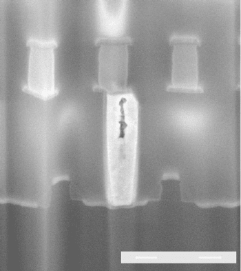
When milling a (single) cross section, it is often important to stop the
polishing step at an exact position in the sample (e.g. through the center
of a unique defect, through the void in a semiconductor plug as shown in
Figure 5.9). This end-point determination can be realized very elegantly using
SPI, since the operator gets continuous and instant feedback about the
polishing process (from an applications point of view, this is the main dif-
ference from serial sectioning). As soon as the feature of interest appears in
the live SEM image, the FIB polishing process is stopped by the operator.
The last step in FIB TEM preparation is to mill a portion of the specimen
thin enough to be electron transparent (e.g., 100 nm or less) [7]. This last
step in the process is conveniently monitored by (i) measuring the specimen
thickness via top-down FIB imaging in conjunction with (ii) monitoring the
remaining thickness of the protecting layer (usually Pt) on the top of
the specimen. When this protective layer starts to recede and approach the
specimen surface, the FIB thinning process should be stopped. SPI mode
proves to be an efficient means to monitor this process (i) without imaging
unnecessarily with the FIB and (ii) to precisely stop the FIB milling at the
appropriate moment. Furthermore, regions that are FIB milled to electron
500 nm
Figure 5.9 Example of an SE SEM image of an FIB milled cross section
through a plug in a semiconductor device. SPI mode was used to determine
the end point of the polishing process, resulting in a cross section through the
center of the plug where the void is located.
Characterization methods using FIB/SEM DualBeam instrumentation 139
transparency for TEM will also exhibit changing contrast as observed with
the SEM. In particular, as the specimen thins, secondary electrons will not
only be emitted from the front surface, but also from the back surface,
resulting in higher SEM contrast levels at the thinnest portion of the speci-
men. SPI mode can be utilized to monitor this contrast change for precise
end-pointing of TEM specimen preparation. Of course, this effect is quite
complex and depends on the energy of the primary electrons, the target
specimen and the relative foil thickness.
The nature of a multi-step process is often advantageous for using SPI
mode. In addition, as the process nears its final steps, a more stringent
requirement for precision using a lower ion beam current usually goes hand
in hand. The former simply justifies the use of SPI, whereas the latter makes
it easier to use SPI mode (e.g., lower FIB current means less interference).
5.4 Scanning transmission electron microscopy (STEM)
characterization in the DualBeam
Even though, strictly speaking, STEM is realized using the electron beam
only (using an SEM in this case), we consider it relevant enough to discuss it
here since the preparation method of choice for STEM imaging is often FIB
or DualBeam. The preparation process and characterization steps may be
combined very elegantly and conveniently in a DualBeam microscope.
We note that for the point of this discussion, STEM refers to SEM-STEM
only, i.e., imaging with 30 keV transmitted or diffracted electrons in an
SEM (or DualBeam). This is clearly different to STEM in a TEM, where
acceleration voltages of hundreds of keV are typically used, and where higher
performance and analytical capabilities are achieved. STEM should not be
considered as a replacement for TEM inspection, but rather (i) as a tool to be
used prior to TEM, (ii) as an aid in TEM specimen preparation and eva-
luation, and (iii) an extension of the conventional SEM and DualBeam. In
particular, it enables SEM operators to capture images with a spatial reso-
lution of less than1 nm.
5.4.1 Preparation of specimens for STEM characterization
STEM specimens are prepared from a bulk material using FIB and DualBeam
techniques that are identical to TEM specimen preparation [7]. Using
DualBeam systems, it is possible to use STEM imaging during the final
thinning of the thin foil. This provides a closed-loop feedback system to the
FIB/DualBeam operator about the thickness and quality of the foil while it is
Focused ion beam systems140
produced. It is possible to use FIB thinning with intermittent STEM inspection,
but on some DualBeam systems, these two steps can even be combined in a
simultaneous process, providing real-time (live) transmission imaging during
the actual thinning using SPI mode.
5.4.2 STEM imaging
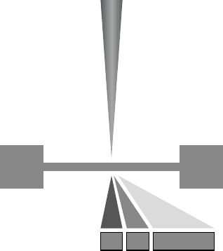
STEM imaging is based on the principle of using a focused primary beam of
electrons that is scanned across a thin specimen. At each point of the scan,
the electron beam interacts with the specimen material, either passing or
diffracting through it. The transmitted electrons are collected on a solid-state
detector. When energetic electrons strike a solid-state detector (usually made
from silicon), electron–hole pairs are formed which produce an electrical
current proportional to the energy of the entering electron. This current is
then amplified in an external electronic circuit, and translated into gray levels
to form an image. The transmission and detection process is illustrated
schematically in Figure 5.10.
Collection of the direct beam yields bright field images (labeled ‘‘BF’’ in
Figure 5.10). Bright field images yield contrast from mass-thickness effects
and diffraction contrast due to crystalline defects in the specimen. The
interaction of electrons with heavy atoms is stronger than with light atoms,
SEM
Thin sample
SS detector
BF DF HA-DF
Figure 5.10 A schematic diagram of the concept of STEM imaging. The
primary electron beam is scanned through a thin sample. Bright field (BF),
annular da rk field (DF), and high-angle annular dark field (HA-DF) signals
can be collected on the respective segments of a solid-state (SS) detector.
Characterization methods using FIB/SEM DualBeam instrumentation 141
so that areas in which heavy atoms are localized appear darker in contrast
than areas with light atoms. In thicker specimen areas, more electrons are
scattered, causing these areas to appear dark. In addition, defects or grains at
different orientations can also scatter the primary beam, causing diffraction
contrast. In principle, FIB prepared STEM specimens have uniform thickness,
so thickness contrast is usually negligible.
For dark field imaging, the opposite result is obtained: heavier and/or
thicker areas will yield a brighter contrast, since more scattering of electrons
occurs and are detected. The scattered electrons are deflected from their
straight paths, and are collected on an off-axis segment, or annular portion of
the detector, labeled ‘‘DF’’ in Figure 5.10. Since defects can also scatter the
primary beam, dark field imaging can enhance features such as crystal
orientation and other crystalline defects.
High-angle dark field detection uses mostly the electrons that are scattered
over the largest angles: this detector segment is placed furthest off-axis. Dif-
fracted beams due to crystalline defects are typically scattered at low angles.
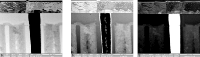
High-angle scattered electrons depend on mass or Z-contrast. Figure 5.11
shows an example of BF, DF, and HA-DF STEM images of the same sample
area. The differences in contrast are evident. In particular, the BF image
shows both mass-thickness effects and diffraction effects. The DF image
shows some reversal of mass-thickness contrast effects compared to the BF
image, but also shows diffraction contrast effects. However, the HA-DF
image shows almost entirely Z-contrast effects; i.e., the heavy W plug shows
the brightest contrast in the image, but some diffraction contrast is also noted.
5.4.3 STEM elemental analysis (EDS)
One of the most appealing features of the SEM(DB)-STEM technique is
the improved spatial resolution that it creates for X-ray energy dispersive
(a) (b) (c)
Figure 5.11 (a) BF, (b) DF, and (c) a HA-DF image of the same sample area
using identical primary beam and scan conditions.
Focused ion beam systems142
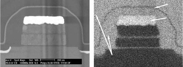
spectrometry (XEDS). Since the specimens are electron transparent, the beam
spread and interaction volume normally associated with bulk SEM samples
will be greatly reduced. Therefore, significantly higher spatial resolution can
be obtained using the STEM detector while performing X-ray analysis.
Typically, a resolution improvement from hundreds of nanometers or even
some micrometers, to about 30 nm can be achieved. It also provides less
background in the spectrum and allows for better separation of peaks as well as
lower count rate mapping conditions. An example of a high-resolution X-ray
map on a semiconductor device is shown in Figure 5.12. A nitride line with
thickness well below 50 nm is clearly resolved in the XEDS map.
5.5 FIB analytical techniques: particle induced X-rays and
secondary ion mass spectroscopy
5.5.1 Focused ion beam induced X-rays (FIBIX)
As previously mentioned, ion–solid interactions yield a complex combination
of particle sputtering and signal generation, among which is the ejection of
characteristic X-rays. This physical phenomenon is the basis for particle
induced X-ray emission (PIXE). PIXE has generally been performed using
light ions or protons accelerated at energies in the MeV range. To distinguish
that FIB induced X-ray analysis is performed with heavy ions of moderate
energy (i.e., 30 keV), we shall use the term FIBIX. FIBIX can be used in a
DualBeam as a complement to SEM based XEDS analysis [8].
The advantages of ion beam induced X-ray emission are twofold. First, the
FIB induced X-rays originate from a region close to the surface of the sample
material – typically not more than a few tens of nanometers deep (e.g., a
N
O
W
(a) (b)
Figure 5.12 (a) DF STEM image and (b) XEDS map of a semiconductor
device showing high-resolution elemental analysis. The arrows indicate the
presence of the respect ive N, O, and W.
Characterization methods using FIB/SEM DualBeam instrumentation 143
smaller interaction volume compared to SEM). Thus, surface analysis or
accurate depth profiling could be achieved. Second, the Bremmstralung is
theoretically orders of magnitude lower. Therefore, ion induced spectra may
provide superior signal to noise ratios over electron beam induced XEDS. A
disadvantage to FIBIX is that a well-defined cut-off energy exists, above
which it is impossible to obtain characteristic X-rays from the target. How-
ever, the technique is most suited for the collection of soft X-rays (< 2 keV),
and is therefore sensitive to light element analysis. As such, FIBIX forms a
good complement to electron induced EDS.
5.5.2 Secondary ion mass spectroscopy (SIMS)
The fundamental process of FIB sputtering is the basis of SIMS. While most
of the sputtered species are neutrals, secondary ions are also emitted. These
secondary ions are detected in an ion mass analyzer such as a quadrupole,
magnetic sector, or time-of-flight (TOF). Correlating the analyzer signal with
the scanning of the ion beam results in ion images with lateral element dis-
tribution. Taking the sputtering yield into account, depth profiles can be
obtained as well. Since FIB process mix a small cascade interaction with a
small probe size, lateral resolution of elemental specific ion images as low as
20 nm may be obtained, while local concentrations of the order of a few
percent can be detected. In comparison, lateral resolution for non-FIB SIMS
ranges from 50 to 200 nm, depending on the primary beam element used.
Ga
þ
ion beams offer a very small probe size and are most widely used in
commercial FIB systems. However, they offer a relatively low yield of sec-
ondary ion production. The secondary ion yield for Ga
þ
is typically about a
factor of 40 less than O
2
þ
, which is used in some non-FIB SIMS equipment [7].
Although superior lateral resolution can be obtained with commercial FIB
instruments, the relatively low secondary ion yield combined with low collec-
tion efficiency in quadrupole mass spectrometers limits the utility of elemental
mapping with FIB-SIMS. Enhancement of the secondary ion yield or detection
efficiency is needed to increase the sensitivity of FIB-SIMS.
5.6 Other opportunities for in-situ characterization
Focused ion beams, and DualBeams in particular, enable further opportunities
for in-situ characterization. Like SEM, FIB enables the use of mechanical
micromanipulators and electrical probes, for characterization of mechanical
and electrical properties, inside the microscope. Furthermore, it is also possible
Focused ion beam systems144
to combine in-situ fabrication or modification of mechanical or electrical
structures with live monitoring of the relevant parameters.
Acknowledgements
Thanks to Hans Mulders and Mark Wall, FEI, for added contributions.
References
[1] D. N. Du nn and R. Hull. Appl. Phys. Lett., 75 (1999), 3414–16.
[2] P. G. Kotula, M. R. Keenan and J. R. Michael. Microsc. Microanal., 9, Suppl. 2,
(2003), 1004–15.
[3] S. Reyntjens. Dualbeam (FIB/SEM) sample preparation for sub-micrometer
EBSD analysis. Presented at Advances in Focused Ion Beam Microscopy: FIB
2003, Cambridge, UK (2003).
[4] M. K. Miller, K. F. Russell and G. B. Thompson. Ultramicroscopy, 102 (2005),
287–98.
[5] J. J. L. Mulders and A. P. Day. Three-dimensional texture analysis. Proc.
ICOTOM 14, Leuven, Belgium (2005), 237–42.
[6] J. J. L. Mulders and H. L. Frazer. Microsc. Microanal., 11, Suppl. 2 (2005), 506–7.
[7] L. A. Giannuzzi, F. A. Stevie, eds., Introduction to Focused Ion Beams:
Instrumentation, Theory, Techniques and Practice (Berlin: Springer, 2005),
pp. 201–28.
[8] L. A. Giannuzzi. Scanning, 27 (2006), 165–9.
Characterization methods using FIB/SEM DualBeam instrumentation 145
6
High-density FIB-SEM 3D nanotomography:
with applications of real-time imaging
during FIB milling
e. l. principe
Carl Zeiss SMT Inc., Redwood City, CA
6.1 Introduction
The ability to acquire, display, and interrogate multi-dimensional volumetric
data sets has been well established through various scientific disciplines. The
medical field in particular has exposed the public to tomographic methods
through now common medical procedures such as computed axial tomo-
graphy (CAT), magnetic resonance imaging (MRI), and positron emission
tomography (PET). In an analogous fashion the focused ion beam (FIB) and
scanning electron microscope (SEM) can combine to generate tomographic
data using the FIB-SEM platform.
Early work completed by a small number of researchers gives an indication
of the variety of information that can be obtained by FIB based tomo-
graphy: Uchick et al. [1] and Kotula et al. [2] have produced secondary
electron (SE) and X-ray images (XEDS) of 3D structures; Dunn et al. [3]
have created 3D mass spectral images using planar FIB etching (FIB-SIMS);
Inkson et al. [4] and Sakamoto et al. [5] have published 3D reconstructions
based on secondary electron images, and Principe [6] has demonstrated the
application of FIB-Auger spectroscopic 3D reconstruction at 10 nm resolu-
tion. Konrad et al. [7] have demonstrated sequential automated acquisition
of 3D electron backscatter pattern (EBSP) tomographic data. This prior
work has shown that FIB based tomographic methods have volumetric data
resolution down to 20 nm or less (i.e., FIB-SE, FIB-Auger) and have tre-
mendous potential for a variety of investigations in both material science and
biology.
Hardware has existed for over a decade to allow collection of volumetric data
from a set of sequential FIB serial sections yet FIB based nanotomography
Focused Ion Beam Systems: Basics and Applications, ed. N. Yao.
Published by Cambridge University Press. ª Cambridge University Press 2007.
146
has until now remained impractical for a routine user. Wider utilization of
FIB based tomographic methods required improvements in the ease of
acquisition, data collection speed, and density of raw data collection.
Advanced FIB-SEM systems such as the CrossBeam family now permit
unattended automated acquisition of volumetric data sets combining XEDS,
EBSP, SE, and backscatter electron (BSE) data. Another enabling factor is
integration of software tools that allow reconstruction, visualization, and
analysis of the data sets including transparency mapping, surface meshing,
exploration of sub-volumes, and animation. This recent evolution in both
hardware and software on FIB-SEM platforms coupled to advanced data
analysis is driving the rapid growth in the field of FIB based tomography by
providing accessibility to the routine user.
With the advent of high-resolution simultaneous secondary electron (SE)
and backscatter electron (BSE) imaging during the FIB sectioning process
on the CrossBeam platform it has become practical to acquire several
hundred data frames in the span of less than one hour in a continuous and
automated fashion for volumes of 500 mm
3
or greater. The approach of
using simultaneous and continuous SEM imaging during the FIB milling
process to create a 3D reconstruction and the method of 3D quantification
described in this chapter was developed and first demonstrated by the
author. Real-time imaging coupled with automated image recording facil-
itates the data acquisition process while providing volumetric resolution at
the nanoscale. High throughput is also a direct result of being able to
capture high quality image data at high density in real-time during the
milling process.
As will be described through the examples presented, the information
content is not limited to powerful visualization and failure analysis; it is a
research tool that can be applied to quantitatively correlate microstructure,
material properties, and system performance. Aspects of data acquisition,
data processing, and quantification will be described.
6.2 Overview of 3D tomography
The word tomography comes from the Greek words tomos (‘‘to cut or sec-
tion’’) and graphein (‘‘to write’’). FIB-SEM nanotomography fits this literal
definition quite well. In this process the sample is sectioned with the FIB and
the result is ‘‘written’’ in the form of digital data. A three-dimensional
reconstruction results when the individual tomograms are arranged in proper
order to reconstruct representation of the original object. The terminology
for a three dimensional digital image element is known as a voxel, which is
High-density FIB-SEM 3D nanotomography 147