Zhang K., Li D. Electromagnetic Theory for Microwaves and Optoelectronics
Подождите немного. Документ загружается.


2.6 Dielectric Layers and Impedance Transducers 111
then the input impedance at the surface of the intermediate medium is equal
to the normal-wave impedance of the input medium and the reflection will
be eliminated:
Z(x
2
) =
Z
2
C
Z(x
1
)
=
Z
Ci
Z
CL
Z
CL
= Z
Ci
and the reflection is vanished,
Γ (x
2
) = 0.
The state of Γ (x
2
) = 0 and ρ = SWR = 1 is know as the state of matching,
i.e., the traveling wave state.
This is known as the quarter-wavelength anti-reflection coating and also
as the quarter-wavelength impedance transducer.
Obviously, the single-section quarter-wavelength impedance transducer is
a frequency sensitive or narrow band device.
2.6.2 Multiple Dielectric Layer,
Multi-Section Impedance Transducer
The bandwidth of a single-section transducer is narrow. To broaden the
bandwidth, we may increase the number of the quarter wavelength sections
to form a multiple dielectric layer or a multi-section impedance transducer.
For a N section transducer, the imp edance relation for the neighboring
sections is
Z
2
Ci
= Z
C(i−1)
Z
C(i+1)
.
The solution of a Multi-section Impedance Transducer is not unique, so
there are a number of designs. The most popular design is the Chebyshev
polynomial design and the binomial design. The former gives a equal ripple
response and the latter gives a flatness response. The design of a multi-
section impedance transducer or a multiple dielectric layer is to be given in
Section 3.7.
2.6.3 A Multi-Layer Coating with Alternating Indices.
The Chebyshev and binomial multi-section transducers are successfully used
in microwave transmission systems. But for microwave or optical coatings,
it may be difficult to find a transparent dielectric material with the required
wave impedance or the required index that adheres well to the substrate.
A multi-layer coating with an alternating wave impedance or alternating
indices, as shown in Fig. 2.26, is much easier to make. It may become an
anti-reflection (AR) coating as well as a high-reflection (HR) coating [38].
The wave impedances of the input and the output media are Z
Ci
and
Z
CL
, respectively. There are a number of layer pairs in between the input
and the output media. The wave impedances of the dielectrics in each layer
pair are Z
C2
and Z
C1
and their thickness is λ/4, where λ is the wavelength
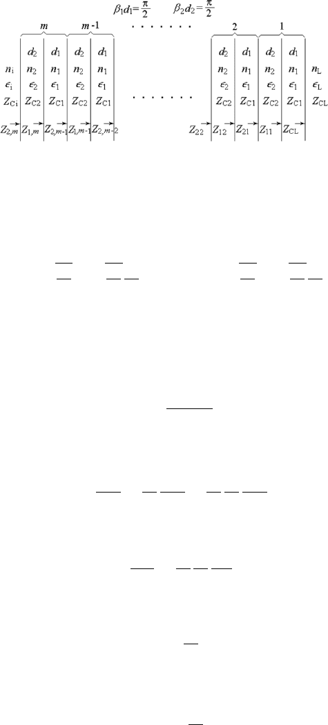
112 2. Introduction to Waves
Figure 2.26: A multi-layer coating with an alternating index.
in the medium or waveguide. Thus we have a multi-layer λ/4 coating with
an alternating wave impedance or alternating index.
Z
C1
=
r
µ
0
²
1
=
r
µ
0
²
0
1
n
1
, Z
C2
=
r
µ
0
²
2
=
r
µ
0
²
0
1
n
2
.
Suppose there are m pairs of layers, i = 1 to m, counted from Z
CL
. The
input impedance of the layer with Z
C1
of the ith layer pair is Z
1i
and the
input impedance of the layer with Z
C2
of the ith layer pair is Z
2i
, which is
the input impedance of the ith layer pair. See Fig. 2.26.
For the first λ/4 layer, referring to (2.259), we have
Z
C1
=
p
Z
11
Z
CL
,
which means that the input impedance of the layer with Z
C1
of the first layer
pair is given by
Z
11
=
Z
2
C1
Z
CL
=
µ
0
²
1
1
Z
CL
=
µ
0
²
0
1
n
2
1
1
Z
CL
.
Similarly, the input impedance of the layer with Z
C2
of the first layer pair is
given by
Z
21
=
Z
2
C2
Z
11
=
µ
0
²
0
1
n
2
2
1
Z
11
.
Substituting the expression for Z
11
into it yields
Z
21
= Z
CL
µ
n
1
n
2
2
.
For the ith pair of layers,
Z
2i
= Z
2,i−1
µ
n
1
n
2
2
. (2.261)

2.6 Dielectric Layers and Impedance Transducers 113
We come to the conclusion that a pair of λ/4 layers transforms the
impedance by multiplying it by the factor n
2
1
/n
2
2
. For a coating system of m
pairs of λ/4 layers on the substrate, the input impedance seen at the input
plane Z
2m
with respect to the impedance of the substrate Z
CL
is given by
Z
2m
= Z
CL
µ
n
1
n
2
2m
=
r
µ
0
²
0
1
n
L
µ
n
1
n
2
2m
. (2.262)
The transformation ratio of the input impedance to the impedance of the
substrate is the 2mth power of the ratio of the indices of the layers. Even
for a ratio n
1
/n
2
very close to unity, the multiplier can be made much larger
or much smaller than unity by choosing the relation between n
1
and n
2
, and
making a large number of layer pairs m.
1. Anti-reflection (AR) coating. For optical elements, n
L
is usually larger
than n
i
. The multiple layer pairs act as an anti-reflection coating if
n
1
> n
2
and m is large enough. The ratio n
1
/n
2
is chosen as
n
i
n
L
µ
n
1
n
2
2m
≈ 1, i.e.,
Z
CL
Z
Ci
µ
n
1
n
2
2m
≈ 1,
so that
Z
2m
= Z
CL
µ
n
1
n
2
2m
≈ Z
Ci
, and Γ =
Z
2m
− Z
Ci
Z
2m
+ Z
Ci
≈ 0.
This is the matching state.
2. High-reflection (HR) coating. The multiple layer pairs act as a high-
reflection coating if m is large enough, n
1
< n
2
, and n
1
/n
2
is chosen
as
n
i
n
L
µ
n
1
n
2
2m
¿ 1, i.e.,
Z
CL
Z
Ci
µ
n
1
n
2
2m
¿ 1,
so that
Z
2m
= Z
CL
µ
n
1
n
2
2m
¿ Z
Ci
and Γ =
Z
2m
− Z
Ci
Z
2m
+ Z
Ci
≈ −1.
This is the high reflection state.
In most applications, the low-loss highly reflecting mirrors made with
multi-layer dielectric coatings are even better than those made with metal-
lic coatings. Of course, the anti-reflection or high-reflection property of a
multi-layer dielectric coating is frequency dependent, because the layers are
a quarter-wavelength thick only at a specific frequency. The band width of
such a multi-layer dielectric coating can b e large enough if the number of layer
pairs is large enough. Usually, the number of layer pairs is up to hundreds
for an optical coating.
114 2. Introduction to Waves
The multi-layer coating with an alternating wave imp edances can also
be analyzed as a DFB structure by means of a periodic system and mode-
coupling theories, refer to Chapter 7.
Problems
2.1 (1) Find the instantaneous Poynting vector of a linearly polarized plane
wave with respect to time and distance.
(2) Prove that the instantaneous Poynting vector of a circularly polar-
ized plane wave is independent of time and distance.
2.2 The expression for an elliptically polarized wave is given as
E = (E
a
+ jE
b
)e
j(ωt−kz)
,
where E
a
and E
b
are not necessarily perpendicular to each other.
(1) Find the relations among E
a
, E
b
and E
xm
, E
ym
, δ
x
, δ
y
in (2.71).
(2) Find the angle between E
a
and E
b
.
(3) Find the condition under which E
a
and E
b
are perpendicular to
each other.
(4) Find the corresponding magnetic field vector H.
2.3 The electromagnetic parameters of earth depend upon the dampness.
For dry earth, ²
r
≈ 5, σ ≈ 10
−5
S/m, and for wet earth, ²
r
≈ 10,
σ ≈ 10
−1
S/m.
(1) Find the frequency for σ = ω² for the above two cases.
(2) Find the depth of penetration of a plane wave at 100 MHz in the
above two cases.
2.4 Calculate the attenuation coefficient, phase velocity, and wave
impedance for a plane wave of frequency 10 GHz propagating in glass.
For typical glass at 10 GHz, ²
0
/²
0
= 6, ²
00
/²
0
= 20.
2.5 Derive the expressions for the phase velocity and group velocity of a
uniform plane wave propagating in a good conductor.
2.6 Prove that the power flow entering a good conductor is equal to the Joule
dissipation in the conductor.
2.7 Derive the expression for the group velocity of a plane wave in a good
conductor.
2.8 Find the group velocity of a plane wave in a conductive medium, If σ, ²
0
and ²
00
of the medium are independent of frequency.

Problems 115
2.9 Pure water is a good insulator, its relative permittivity is 81. Find the
power ratio of the reflection wave to the incident wave and that of
the transmission wave to the incident wave, for an incident plane wave
passing normally through the plane surface of the water.
2.10 A plane wave is normally incident upon an boundary between two non-
magnetic, lossless media. Find the condition under which the reflection
coefficient and the transmission coefficient are equal to each other.
2.11 A plane wave with circular frequency ω is incident normally from vac-
uum upon the plane surface of a nonmagnetic conductive medium with
conductivity σ and permittivity ².
(1) Find the reflection coefficient and the transmission coefficient.
(2) Find the reflection coefficient and the transmission coefficient for a
low-loss conductive dielectric and a good conductor. Show that the re-
flection coefficient of a good conductor is given by Γ ≈ 1 −
p
2ω²
0
/σ =
1 − ωδ/c.
2.12 Give the expressions for instantaneous values of the composed field
components for the oblique reflection of n wave and p wave at an air –
perfect conductor plane boundary.
2.13 Find the complex and instantaneous Poynting vectors in the direction
parallel and perpendicular to the boundary for the oblique reflection of
n wave and p wave at an air – perfect conductor plane boundary.
2.14 A light beam is incident from the air upon a nonmagnetic medium of
index n, show that
n
2
=
(1 + Γ
TM
)(1 − Γ
TE
)
(1 − Γ
TM
)(1 + Γ
TE
)
.
This is an experimental method for measuring the index of the dielectric
material. In practice, the incident angle is chosen to be 45
◦
. Note that,
both Γ
TM
and Γ
TE
are negative for an incident angle of 45
◦
, and the
measured values are the power reflection coefficients, hence the negative
square roots of them must be taken for the calculation.
2.15 Show that Fressnel’s formulas for nonmagnetic dielectric media may be
expressed by the following form, in which only θ
i
and θ
t
are included.
Γ
TE
= −
sin(θ
i
− θ
t
)
sin(θ
i
+ θ
t
)
, T
TE
=
2 cos θ
i
sin θ
t
sin(θ
i
+ θ
t
)
,
Γ
TM
=
tan(θ
i
− θ
t
)
tan(θ
i
+ θ
t
)
, T
TM
=
2 cos θ
i
sin θ
t
sin(θ
i
+ θ
t
) cos(θ
i
− θ
t
)
.
116 2. Introduction to Waves
2.16 Prove that for the boundary between magnetic media, i.e., ²
1
= ²
2
and
µ
1
6= µ
2
, the Brewster angle exists only for the TE wave. Find the
expression for the corresponding Brewster angle.
2.17 Derive the composed field expressions for the TM mode in the case of
total reflection.
2.18 (1) Calculate the critical angle for a plane wave passing from pure water
into air, for the pure water, ²
0
/²
0
≈ 81.
(2) Calculate the critical angle for a plane wave passing from glass into
air, for typical glass, ²
0
/²
0
≈ 6.
2.19 (1) Calculate the Brewster angle for a plane wave passing from from
air into pure water and from pure water into air.
(2) Calculate the critical angle for a plane wave passing from air into
glass and from glass into air.
2.20 In the case of total reflection,
(1) Prove that the average active Poynting vector along the direction
perpendicular to the b oundary is zero, both in the incident region and
the refraction region.
(2) Find the Poynting vector and the power flow per unit width along
the direction parallel to the boundary.
2.21 Reflection mirrors for the HeNe laser consist of alternative coatings of
ZnS and ThF
2
. The refractive indices of them are 2.5 and 1.6, respec-
tively. The index of the substrate is 1.5 (glass). Find the minimum
number of layer pairs for a p ower reflection coefficient greater than
99.5%. The wavelength of the HeNe laser beam is 632.8 nm.
2.22 When a plane wave is reflected from the boundary of a dielectric,
(1) under what condition does the circularly polarized incident wave
becomes linearly polarized reflected wave.
(2) under what condition does the linearly polarized incident wave be-
comes a circularly polarized reflected wave.
Chapter 3
Transmission-Line Theory
and Network Theory for
Electromagnetic Waves
Two powerful tools based on circuit theory, transmission line theory and
network theory, are widely applied to the analysis and simulation of var-
ious electromagnetic wave phenomena. In this chapter, the basic concept
of distributed circuits, the waves propagating along transmission lines, the
transmission-line charts, the elementary network theory and the impedance
transducers are introduced.
3.1 Basic Transmission Line Theory
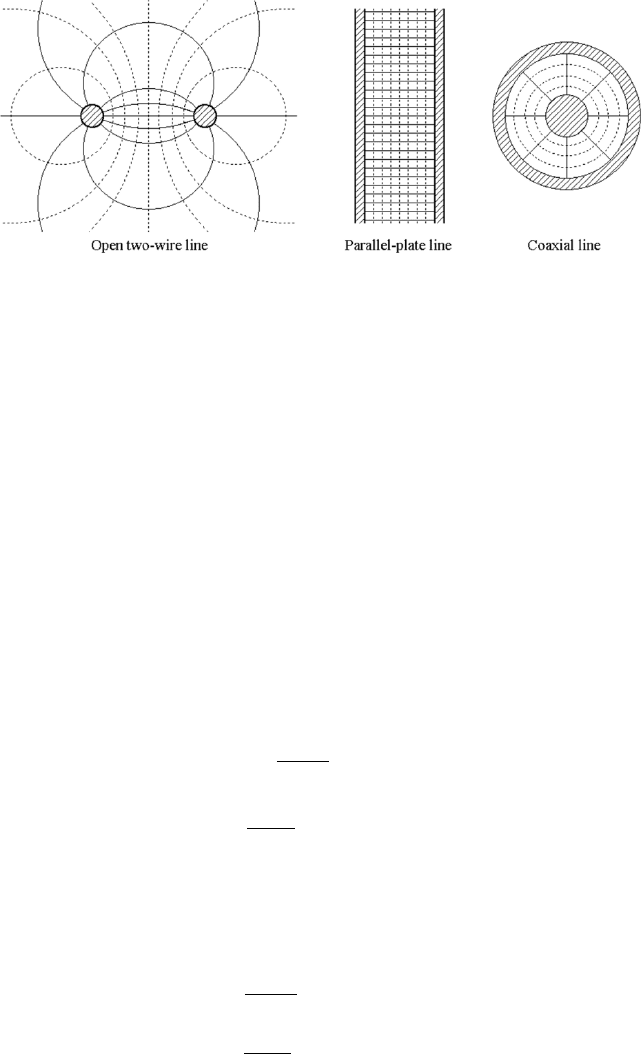
A transmission line made up of two parallel wires is the earliest system for
the transmission of electromagnetic signals and energies. In general, a trans-
mission line may be made up of any two conductors separated by a dielectric
insulator, for example, parallel wires, parallel plates, or coaxial conductors,
see Figure 3.1. For a transmission line with two conductors, the boundary
conditions can be satisfied by TE, TM and TEM modes. Among them, TEM
mode is the dominant mode.
Two different approaches are used in the analysis of the TEM wave in
transmission lines, the field approach and the circuit approach. In the field
approach, we deal with the field distribution in a specific transmission-line
structure, and the result can be used for only this specific structure. In
the circuit approach, distributed circuit parameters are introduced and the
transmission line can be described as a distributed-parameter electric net-
work. The result of the circuit approach is suitable for transmission lines
of any structure, and the circuit parameters for a specific structure can be
118 3. Transmission-Line and Network Theory for Electromagnetic Waves
Figure 3.1: Transmission lines.
formulated by means of static field theory.
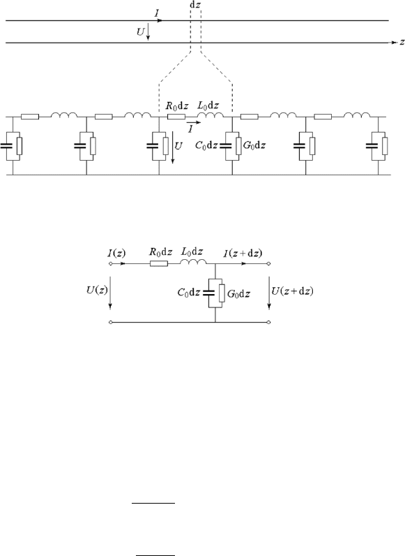
3.1.1 The Telegraph Equations
In the circuit approach, the transmission line can be described as series-
connected inductance and resistance per unit length, denoted by L and R, re-
spectively, and shunt-connected capacitance and conductance per unit length,
denoted by C and G, respectively. These circuit elements are not connected
at discrete points on the line, but are distributed infinitesimally along the
line. The transmission line can then be described as a cascade connected
network chain comp osed of a infinite number of differential lengths dz, see
Fig. 3.2. The equivalent circuit for these infinitesimal segments of line is
shown in Fig. 3.3, it consists of circuit elements Ldz, Rdz, Cdz and Gdz.
According to Kirchhoff’s law, the circuit equations for the equivalent cir-
cuit of a differential segment, refer to Fig. 3.3, are written as follows:
U(z + dz) − U(z) =
dU(z)
dz
dz = −(R + jω L )dz I(z), (3.1)
I(z + dz) − I(z) =
dI(z)
dz
dz = −(G + jωC)dz U(z + dz). (3.2)
Let
Z = R + jωL, Y = G + jωC, (3.3)
and neglect the terms including the square of the infinitesimal quantity dz,
gives
dU(z)
dz
= −Z I(z), (3.4)
dI(z)
dz
= −Y U (z). (3.5)
3.1 Basic Transmission Line Theory 119
Figure 3.2: Equivalent network with distributed parameter.
Figure 3.3: Equivalent circuit for a differential segment.
These are the transmission-line equations. The forms of these equations are
the same as the one-dimensional source-free Maxwell equations for a plane
wave (2.8) and (2.10) as shown in Section 2.1.
Taking the derivative of equation (3.4) then substituting equation (3.5)
to cancel I(z), yields
d
2
U(z)
dz
2
− Y Z U(z) = 0. (3.6)
Similarly, we have
d
2
I(z)
dz
2
− Y Z I(z) = 0. (3.7)
These two differential equations are known as telegraph equations.
3.1.2 Solution of the Telegraph Equations
We can see that the telegraph equations are just the same as the one-
dimensional scalar Helmholtz’s equations (2.14) and (2.15). The solutions
of (3.6) and (3.7) must be the same as (2.18) and (2.19):
U(z, t) = U(z)e
jωt
=
¡
U
+
e
−γz
+ U
−
e
γz
¢
e
jωt
, (3.8)
I(z, t) = I(z)e
jωt
=
¡
I
+
e
−γz
+ I
−
e
γz
¢
e
jωt
, (3.9)
120 3. Transmission-Line and Network Theory for Electromagnetic Waves
where
γ = α + jβ =
√
Y Z, (3.10)
is the propagation factor of the wave; the real part is the attenuation factor
and the imaginary part is the phase factor.
Substituting (3.8) into (3.4), yields
I(z, t) = I(z)e
jωt
=
µ
U
+
Z
C
e
−γz
−
U
−
Z
C
e
γz
e
jωt
, (3.11)
where
Z
C
=
U
+
I
+
= −
U
−
I
−
=
Z
γ
=
r
Z
Y
, (3.12)
denotes the characteristic impedance of the transmission line which is the
ratio of the voltage to the current of a traveling wave and is determined by
the configuration of the transmission line [24].
(1) The General Case
In the general case, the propagation factor and the characteristic impedance
are complex,
γ = α + jβ =
p
(R + jωL)(G + jωC),
where
α =
r
1
2
h
p
(R
2
+ ω
2
L
2
) (G
2
+ ω
2
C
2
) − (ω
2
LC − RG)
i
, (3.13)
β =
r
1
2
h
p
(R
2
+ ω
2
L
2
) (G
2
+ ω
2
C
2
) + (ω
2
LC − RG)
i
, (3.14)
and
Z
C
=
r
Z
Y
=
s
R + jωL
G + jωC
. (3.15)
It is just the same as the plane wave in a lossy medium. There are two
attenuated traveling waves propagate on the transmission line with opposite
directions of propagation.
(2) Low Frequency, Large Loss
In the case of relatively low frequency and relatively large loss,
ωL ¿ R, ωC ¿ G.
We have
α ≈
√
RG, β ≈ 0.
There is no wave propagation, only attenuation on the line.