Yao N. Focused Ion Beam Systems: Basics and Applications
Подождите немного. Документ загружается.

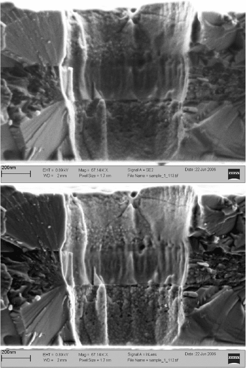
working distance with an original screen magnification of 215 000 · (67.14k ·
in 4 · 5 format) and a field width of 1.7 m m. Using dual channel mode both
images were acquired simultaneously during a single scan where the image in
Figure 6.4(a) was captured on the Everhart–Thornley SE detector and
the image in Figure 6.4 (b) was recorded using the in-lens SE detector. As
both images were acquired simultaneously under identical primary beam
(a)
(b)
Figure 6.4 Semiconductor cross section image acquired at 890 eV at an
original screen magnification of 215 000 · and a horizontal field width of
1.74 mm. Both images were acquired simultaneously under identical beam
conditions. Panel (a) was recorded with the Everhart–Thornley detector and
panel (b) was recorded with the in-lens SE detector. The improved
resolution in the lower in-lens image is due to emphasis on SE
1
detection
and the reduced contri bution of SE
2
and SE
3
image signals.
Focused ion beam systems158
conditions the images compare the character of the different signals captured
by the two detectors. The signal-to-noise ratio is somewhat lower in the ET
image relative to the in-lens image due to the short working distance. It is
clear that the in-lens detector reveals greater detail and improved resolution
with respect to the ET detector. This example visually illustrates the effect of
electron–solid interactions discussed above and the difference between a high
spatial resolution SE
1
in-lens detection signal and an ET detector convolved
with a contribution of SE
2
and SE
3
signals in the image. In the 3D recon-
struction application we will primarily employ the in-lens detectors to take
advantage of the superior spatial resolution.
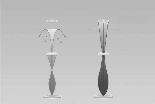
Low voltage on-axis in-lens energy selective backscatter (EsB) detection
The principle of on-axis in-lens electron projection detection is extended to
partition and extract low energy BSE
I
from SEs. The following discussion is
with reference to Figure 6.5. It is possible to separate the BSE
I
signal from
SEs and BSE
II
electrons because the BSE
I
are distinct both in terms of energy
distribution and trajectory distribution. Secondary electrons pass through an
electrostatic focus and diverge en route to the on-axis in-lens SE detector,
as shown on the left-hand side of Figure 6.5. A small number of secondary
electrons pass through the annular opening in the SE detector and are
repelled by an adjustable field generated by an electrostatic grid. Low loss
BSE
I
electrons which follow a nearly axial trajectory pass through the annular
EsB detector
BSE
SE
In-lens SE
detector
Filtering
grid
SE detection
BSE detection
Figure 6.5 Schematic representation of the electron projection paths defining
the in-lens SE detection and in-lens EsB detection. Secondary electro ns are
projected onto the in-lens SE detector while the BSE
I
follow an axial
projection onto the upper in-lens energy selective backscatter detector.
High-density FIB-SEM 3D nanotomography 159
portion of the in-lens detector, shown on the right-hand side of Figure 6.5.
Those BSEs with energy higher than the grid voltage navigate across the field
and are directly detected by the EsB detector. The grid voltage is not only
used to reject secondary electrons but it is also an energy filtering element
that can be used to create an energy window between the primary and grid
voltages. Using this type of BSE
I
detection system it is possible to collect a
low voltage high spatial resolution z-contrast image at short working distance
with a 25 eV energy image window. Isolating the BSE
I
signal at low voltage
coupled with energy filtering to concentrate on the elastic peak is a benefit in
3D reconstruction.
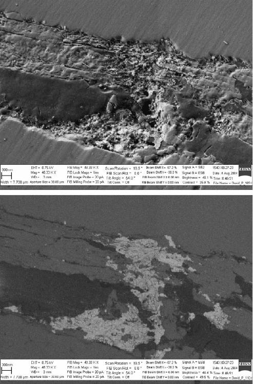
High scattering angle BSE
I
images will also display minimum topography in
addition to strong material contrast, as illustrated through the image pair in
Figure 6.6. The sample is an uncoated geological material. The images were
acquired at 750 V with a horizontal width of 7.7 m m. Both images in Figure 6.6
were acquired simultaneously during a single scan and captured using two
detectors. The side chamber mounted SE
2
detector was used to collect the
image shown in (a) and the energy selective backscatter (EsB) detector was
used to collect the image in (b). The SE
2
detector image shows strong topo-
graphic contrast while the EsB image displays minimum topography and
strong z-contrast, in a dramatic example of the different information content
extracted by the two detectors. Other contrast mechanisms such as Schottky
barrier contrast, voltage contrast and charging contrast are also suppressed
from an EsB image. Enhanced z-contrast with minimum topography is a
benefit in FIB-SEM 3D reconstruction to separate different materials and
phases throughout the 3D volume during data reduction. Similarly, the elim-
ination of edge contrast, charging contrast, and other contrast mechanisms
deleterious to FIB-SEM nanotomography is also a significant benefit. The
ability to extract this information at low voltages of 1 kV and less means that
depth resolution is also optimized. Moreover, this type of in-lens BSE detector
requires no insertion, alignment, or adjustment. Thus, in many respects the in-
lens EsB is an ideal detector for the purposes of FIB-SEM 3D nanotomo-
graphy. It is expected that future work will continue to highlight the benefits of
FIB-EsB nanotomography in both materials science and emerging biological
applications.
Electrostatic–electromagnetic objective lens
The Gemini column derives it name from the ‘‘twin’’ element configuration of
the objective lens. With attention to Figure 6.3(b), the upper portion of the
objective lens is an electromagnetic element while the lower portion of the
objective lens is an electrostatic element. Collectively, these elements combine
Focused ion beam systems160
to produce the electron optical analogy of an achromatic lens triplet,
represented schematically in the lower right portion of Figure 6.3 (b). The first
lens of the triplet is an electromagnet element and the final two lenses of the
triplet are electrostatic. Traditional electron optics systems consisting only of
focusing elements lead to a lens system with positive aberration coefficients.
(a)
(b)
Figure 6.6 Comparison of images acquired simultaneously on an EsB
CrossBeam highlighting the difference in information content from an SE
2
detector and an in-lens BSE detector. The images were acquired at 750 V
and collected simultaneously using two different detectors. The image
depicted in (a) was formed by the side chamber mounted SE
2
detector and
shows strong topographic co ntrast. The lower image (b) produced with the
in-lens EsB detector displays minimum topographic contrast and strong
z-contrast.
High-density FIB-SEM 3D nanotomography 161
However, the action of the decelerating electrostatic field functions as a
negative aberration lens, represented by the central element of the triplet. The
final electrostatic lens element is the pole piece focusing element. This unique
objective lens design leads to excellent low energy performance because the
chromatic and spherical aberration coefficients actually decrease with pri-
mary electron voltage.
Real-time SEM imaging during FIB milling
The electrostatic component of the Gemini objective lens results in the
absence of any appreciable magnetic field at the sample surface and this leads
directly to a unique ability to image in real-time at ultra-high-resolution
during the FIB milling process. Blurring and beam distortion result during
any attempt to simultaneously operate a gallium FIB column and an SEM
column in the presence of a magnetic field. This interference is due to
interaction between the magnetic field with the isotopes and multiply charged
ions within the gallium ion beam. The electrostatic elements on the lower
portion of the Gemini objective lens contain the vast majority of the elec-
tromagnetic field generated by the upper portion of the objective lens,
creating an opportunity for operation of simultaneous focused ion beam
milling and scanning electron beam imaging.
Another notable consequence derived from the ability to simultaneously
image with the SEM during the FIB milling process is the formation of a
hybrid contrast mechanism that combines the SE image contrast produced by
the primary electron beam and the channeling contrast produced by the ion
beam on crystallographic samples. This operation mode is often desirable
due to strongly enhanced orientation contrast that complements the electron
beam induced SE contrast in the collected image. This hybrid contrast is only
present while both beams are operating simultaneously.
It should be also noted that the real-time imaging during the ion milling
process will not influence the BSE image contrast generated by the primary
electron beam because ion bombardment does not produce backscatter
electrons. Therefore collecting the in-lens EsB signal can also be advanta-
geous when it is desired to suppress orientation contrast. Dual channel
operation allows the operator access to display both these signals simulta-
neously on two separate computer screens during the milling operation.
6.4 Data acquisition parameters for FIB-SEM 3D reconstruction
The preceding established a rationale for using low voltage operation in
order to optimize depth resolution and a strategy to extract SE
1
and BSE
I
Focused ion beam systems162
information content to achieve high-resolution FIB-SEM nanotomography.
Electron detection principles that allow ultra-high-resolution imaging at low
voltage and simultaneous collection of both in-lens SE and in-lens BSE
I
signals have been described. Finally, high density data collection of these
signals is facilitated by the ability to image in real-time during the FIB
milling process by taking advantage of the electrostatic objective lens
design.
The following is a general guideline for data specific acquisition parameters
described for various types of FIB-SEM 3D reconstruction including
FIB-SE, FIB-BSE, and FIB-EBSD. Obviously there are nuances to the
techniques and methods described and the analyst is encouraged to adapt the
methods described here according to their own circumstances. In practice,
once the operation parameters are considered acquisition is executed with
relative ease by an operator oriented with both SEM and FIB instrumenta-
tion. The setup process can also be assisted through a computer-aided expert
system to facilitate the automated procedure.
6.4.1 Electron beam imaging current
An important parameter under the operator’s control to affect the signal-to-
noise ratio in the recorded image data is the electron probe current. The
Gemini column does not suffer the same tradeoff between probe current and
probe size as encountered with a traditional electron column. The details are
related to the lack of crossover in the beam path and the fact that ‘‘spot size’’
is not adjusted by changing the condenser lens setting as on a system with
crossover electron optics. So it is possible to maintain high resolution and
high current while enhancing depth of focus. The high current/high depth of
field mode on the Gemini column approximately doubles the current while
also increasing the depth of field due to a commensurate reduction in the
convergence angle. Therefore, the high current mode is generally a good
choice for a given aperture as an increased depth of field is a benefit that is in
addition to improved signal intensity. Probe currents can be in the range of
less than 10 pA to greater than 20 nA, as desired. Software also allows an
option to automatically track working distance during the milling process to
maintain focus over large cut depths.
The real-time SEM imaging conditions during ion milling used to produce
the 3D reconstruction data in most of this work yielded an incoming count of
approximately 20 000 electrons averaged per pixel per frame and represents a
moderate current. The calculations are derived from the dwell time per pixel,
the probe current, and the frame averaging parameters.
High-density FIB-SEM 3D nanotomography 163
6.4.2 FIB milling current
The FIB milling current will dictate the quality of the cut face and the
amount of time required to mill the selected volume. The current and dwell
time of the ion beam should be designed to ensure that each milling element
cuts completely through all materials in the cross section to the desired depth.
A ‘‘mill to depth’’ option allows a cut depth to be numerically input. The
milling calculation is based upon a materials file that calibrates milling rates
derived from measured or theoretical values input by the user.
The amorphous damage depth due to the milling process is usually not an
issue for SEM imaging. However, be aware of the amorphous damage layer
associated with the FIB milling process and ion beam sensitivity of the
material. A lower FIB voltage will reduce the amorphous depth while
a reduced milling current may reduce the damage rate, particularly on
organic or biological specimens. Amorphous damage is a potential issue
when collecting FIB-EBSD tomographic data. The analytical volume of
EBSD is estimated to be in the range of 30 nm and good EBSD have been
generated from 30 kV FIB using a 2 nA beam. However, the analytical
volume of the EBSD data and the tolerable range of amorphous damage will
be highly material dependent and even grain orientation dependent. In the
case of FIB-EBSD it is most practical to run tests to confirm good quality
patterns for a given FIB milling current.
An acceptable current range for FIB-SEM data collection can be anywhere
from 10 pA–20 nA. The specific ion beam current will depend upon the
milling properties of the material, the physical volume of the data cube and
the time allotted for the acquisition. Assuming a nominal data volume
consisting of 10 mm in width (x-axis), a z-depth of 5 mm and a y-depth of less
than 10 mm, the acquisition can be completed in approximately one hour or
less on a silicon based material with a current of 20–50 pA (recall with
reference to Figure 6.1, that the z-axis represents the axis along which the
cutting plane (x–y plane) will advance).
6.4.3 Acquisition time
One hour is quite reasonable for the typical sample volumes of approximately
500 mm
3
, but there is no serious compromise associated with longer acqui-
sition time. Some FIB-EBSD experiments have operated continuously for up
to four days. Sample drift also is not an issue since the data set requires image
alignment even with zero image drift, as described in the data reduction
section. In sequential acquisitions, as in FIB-EBSD and FIB-XEDS, automatic
Focused ion beam systems164
image registration is employed between data acquisition cycles for both FIB
and SEM alignments.
6.4.4 Image collection frequency
The depth resolution along the cutting plane has been estimated as 5–20 nm
while the data acquisition time has been defined as 3600 seconds. Together
with knowledge of the linear dimension along the cutting plane (x–y plane
and z-axis, with reference to Figure 6.1) it is possible to determine the
appropriate image acquisition rate. It is a good practice to acquire the data at
a slice thickness that corresponds to half the estimated resolution limit.
Assuming a 20 nm depth resolution, an image will be collected every 10 nm.
Assuming this 10 nm value and a linear z-axis dimension of 1.5 mm, the
number of required frames is 150. The total number of required frames to
achieve a 10 nm resolution in this example corresponds to an image recorded
every 24 seconds. Using the frame averaging noise reduction mode the system
can automatically average approximately 200 frames every 20 seconds. It is a
sound practice to collect an image at twice the frame averaging cycle rate.
Continuing with this example, collecting an image every 10 seconds yields
a 4 nm slice thickness and a total of approximately 350 frames. In this
instance the data acquisition parameters are such that we are over sampling
by nearly a factor of three to five relative to the estimated resolution limit. In
the data reduction process one may choose to work with all the data frames
or cull the data using any index parameter, i.e., every other frame. Thus, in
general, an image recorded every 10–20 seconds will produce a high quality
FIB-SEM nanotomographic reconstruction at a 10–20 nm resolution over
volumes of 250–500 mm
3
.
If very high milling rates are desired for milling larger volumes or smaller
volumes in a shorter time period then faster AVI capture rates may be used.
The system software on the CrossBeam has a built-in AVI capture capability
that allows the images to be recorded as frequently as every 100 ms.
6.4.5 Pixel size
The image pixel size is a function of both the SEM magnification and the
image store resolution. At a screen magnification of 10 000 · it is reasonable
to employ a 1 K · 1 K store resolution but it is possible to save the images at
a3K· 2 K store resolution. It is interesting to note that the maximum
achievable resolution can be recorded without any a priori knowledge of the
structures contained in the data volume. Following data acquisition it is of
High-density FIB-SEM 3D nanotomography 165

course possible to post-process any sub-volume of interest and digitally zoom
in on any feature in the volume, but that operation won’t ultimately increase
the information content contained in the data.
6.4.6 Storing images
The storage volume required will depend upon the number of AVI movies
recorded over time, the store resolution, and the length of those movies.
A typical movie will require 200–300 Mb of disk storage and a comparable
amount disk space for post-data reduction files. As a practical matter it is a
good idea to have a separate storage volume to accommodate the movie data
if one intends to complete a large number of reconstructions, process the
data, and create inspiring animations. Fortunately, data storage is cheap.
6.5 Quantification of FIB based 3D tomographic data
The continuous nature of the milling process, in combination with a method
devised to determine the slice thickness between image frames, facilitates
direct quantification [15]. The continuous nature of the process also means
that the data slices are more uniform in nature and less subject to thickness
variation, charge fluctuation, and re-alignment errors associated with stop-
ping and restarting the tomographic slice process.
The procedure involves patterning one or more features into or on the
surface of the region of interest that can also be viewed in cross section during
the FIB tomographic process. This feature may be etched into the surface by
either the FIB itself or by another means. The feature could also be deposited
onto the surface through the FIB or other method. In other words, the feature
(s) can be either recessed (i.e., etched into) or raised (i.e., deposited) with
respect to the sample plane. If deposited, the pattern can consist of any suitable
material such as an oxide, metal, organic, inorganic, or any combination
thereof. The feature must simply have a known geometric relationship between
the top view and the cross section. The most direct example is a pattern
consisting of at least two straight lines forming a known angle etched into the
surface perpendicular to the cross section, as depicted in Figure 6.7.
Since the angle defined by the lines is known, a mathematical relationship
can be established that is generally described by:
4t
n
¼ L
n
A
n
A
nþ1
A
n
8
>
:
9
>
;
¼
A
n
A
nþ1
tan
8
>
:
9
>
;
ð6:2Þ
Ontheright-handsideofFigure6.7 is an image showing actual fiducial lines
etched into a platinum protective layer on top of a multilayer semiconductor
Focused ion beam systems166
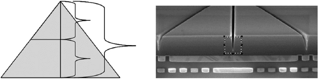
device. As the cut face progresses the angled line(s) move toward the center
line. If the angle is 45
then the change in distance between the center line and
the angle line is equal to the slice thickness. This fiducial system allows
quantification through the mathematical relation above based upon either
the average image slice thickness over the entire acquisition or the thickness
of individual image slices. The ability to image the quantitative mark on the
cross section in a single view improves speed and accuracy of the data.
The data can be processed after the image data acquisition and do not require
any prior knowledge of sample sputter rates (or other properties of the
samples) nor a calibration or measurement during the data acquisition pro-
cess. The fiducial marks are not seen in the processed final data set as they are
usually placed to one side of the image just outside the region.
6.6 Data reduction
The typical steps involved in data reduction are summarized as follows:
(i) image alignment; (ii) selection of the sub-volume representing the region
of interest from the original data volume; (iii) image processing (optional);
(iv) reconstruction of the volume; (v) any additional volumetric analyses
(i.e., porosity, phase density, etc.); (vi) volume visualization, which could
include application of color and transparency mapping; and (vii) animation
of the results as desired.
As mentioned above, image alignment is required even if there is no sample
drift because the image plane is translating in the þy-direction in the SEM
view as the cutting plane progresses. This geometric effect occurs because the
A
1
A
2
L
2
L
1
Dt
u
Figure 6.7 The geometrical relationship above is applied to quantify the
average slice thickness in each frame of the FIB-SEM reconstruction
volume. On the left is a schematic related to Eqn. ( 6.2). On the right is an
example of the fiducial lines etched using the FIB into a platinum layer
created using the deposition capabilities of the FIB. The dashed box around
the central fiducial line is used to perform automated image stack alignment.
As the cut face progresses the angled lines move toward the central line
allowing quantification of the slice thickness based upon the known
geometrical relationship.
High-density FIB-SEM 3D nanotomography 167