Yao N. Focused Ion Beam Systems: Basics and Applications
Подождите немного. Документ загружается.

within the crystallographic lattice. The band width is proportional to the lattice
spacing. The intersection of the several bands represents a zone axis. Collec-
tively, the Kikuchi pattern contains information on the interplanar angles in
the crystal and its orientation. The spatial resolution of the technique is on the
order of 10–20 nm under ideal conditions with a field emission microscope
while the information depth is material dependent and of the order of 30 nm.
In addition to grain orientation, crystal phase, and crystallographic texture the
EBSD patterns are sensitive to strain and lattice deformation.
In order to apply the EBSD technique in 3D it is necessary to address
issues of sample preparation and geometry. Preparation of the surface is
typically a stringent requirement in EBSD because the quality of the patterns
produced is highly sensitive to the morphology and amorphous damage
depth. If the residual damage from mechanical polishing or other preparation
is too severe no patterns will result. Electropolishing is often employed as a
final preparation step to yield a smooth surface with minimum damage.
Using the FIB it is possible to generate a suitably smooth surface for high
quality EBSD patterns. However, it is still important to properly prepare the
sample prior to FIB and that will often require mechanical polishing, but for
reasons primarily associated with geometry rather than surface finish. With
reference to Figure 6.15 the EBSD pattern can only be produced if there is a
line of sight from the sample surface to the camera. One method to meet this
requirement is to create the FIB cut on the edge of a sample. If an FIB cut is
made too far into the interior of the specimen then most of the cut face will be
blocked from the EBSD camera and, unless very large cuts are made, only a
very small area from the top of the cut face will generate an EBSD pattern.
Aside from locating the FIB cut at the edge it is also very helpful to work on
a polished edge. A smooth and polished edge minimizes the amount of FIB
milling time required to mill away rough edges prior to beginning the actual
3D FIB-EBSD. Once a suitable sample is produced it can be mounted and
set up for the automated FIB-EBSD acquisition.
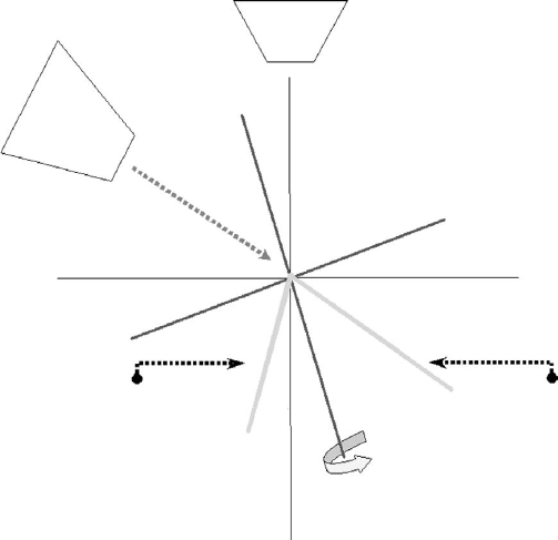
The schematic in Figure 6.16 shows the electron beam, FIB, and sample
geometry for generating 3D FIB-EBSD data on the standard CrossBeam
hardware configuration. For the FIB-EBSD technique the sample will oscillate
between two positions, as shown in Figure 6.16. One position is the FIB
milling position, designated position A and the second position is the EBSD
data collection position B. However, instead of producing an FIB cut normal
to the sample surface at 54
tilt, a cut face is generated with the sample stage
tilted at 17
. Alternatively, a 17
pre-tilt holder may be used. After the sample
is mounted with a smooth edge perpendicular to the stage and the stage is tilted
at 17
the user then selects the area of interest and the volume to be analyzed
Focused ion beam systems178
with the aid of a setup wizard. A fiducial mark (i.e., an ‘‘X’’) is milled into an
appropriate location on the sample surface next to the analysis region and the
location is recorded by the FIB image registration routine. This is the FIB
milling position (position A). The stage is then rotated 180
about the same 17
tilt axis into position B and that location is recorded by the SEM image
registration. As illustrated in Figure 6.16, the geometry dictates that the cut
face is now oriented properly for acquisition of the EBSD data.
The user is guided through the remainder of the setup process including the
EBSD parameters and then the automated routine is initiated. The system will
mill the selected area then rotate into position B and collect the EBSD data and
then return to position A and begin milling the next data slice. This process
repeats until the volume is completed. The time overhead transitioning between
the two stage positions is less than 20 seconds, allocating most of the time to the
EBSD acquisition. The milling time will depend upon the volume to
be analyzed. Very large acquisitions have run continuously for up to four days.
Cone of back-
scattered electrons
Interaction volume
beam sample
Sample
Beam
inclination
~20˚
Electron beam
Diffraction
pattern
Objective
lens
Camera with
phosphor
screen
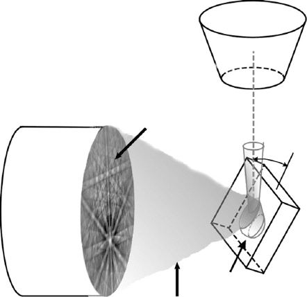
Figure 6.15 Schematic showing the electron beam and sample geometry for
EBSD. The electron beam forms an angle of approximately 20
with the
sample plane. The glancing angle geometry of the electron beam facilitates
production of strong intensity electron channeling patterns (commonly
called electron backscatter diffraction patterns) which escape from the near
surface region of the sample. The projected patterns that are captured on a
phosphor screen form a family of Kikuchi bands that contain crystal-
lographic information from the sample.
High-density FIB-SEM 3D nanotomography 179
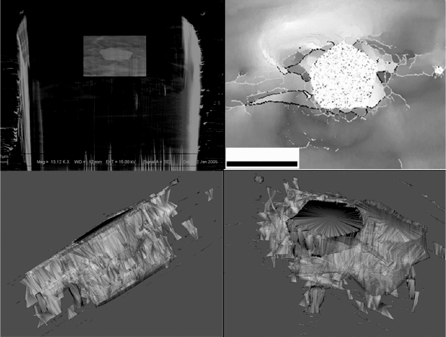
The example shown in Figure 6.17 is taken from the work of Konrad et al.
described in [ 7]. The analysis was conducted on the area surrounding a
hard particle (laves) in an Fe
3
-Al alloy. The purpose of this study was to
characterize the strong orientation gradients surrounding the hard particle
produced during the warm rolling process. Figure 6.17(a) shows the cut face
where the highlight area is the approximate region from which the 3D
reconstruction was completed. The hard particle is the bright area in the
central portion of the region of interest. Figure 6.1 7(b) shows an inverse pole
figure generated from one slice of the EBSD data stack showing the hexagonal
particle in the center surrounded by four orientation gradient zones developed
during rolling. Note the EBSD data is tilt corrected. Figures 6. 17 (c ) a nd (d )
depict the 3D rendering of the EBSD data showing large angle grain boundaries.
There is an exception to the general rule stated earlier that a low voltage is
required to achieve good depth resolution. The explanation to this exception is
Cut face created in
position (A)
Position (B) the cut face is in
EBSD position after 180˚
stage rotation
20˚
17˚
37˚
36˚
17˚
17˚
17˚
Ion
beam
Ebeam
Figure 6.16 Schematic showing the electron beam, FIB and sample
geometry for generating 3D FIB-EBSD data on the standard CrossBeam
hardware configuration. Instead of producing an FIB cut normal to the
sample surface at 54
tilt, a cut face is generated with the sample stage tilted
at 17
. Alternatively, a 17
pre-tilt holder may be used. This is the FIB
milling position designated as position A. After the cut face is created the
stage is rotated 180
about the tilt axis into position B. The geometry
dictates that the cut face is now oriented properly for acquisition of the
EBSD data.
Focused ion beam systems180
related to both the electron beam–sample geometry and electron detection
schemes. When forward scattered low loss electrons are collected using an
appropriate beam–sample geometry and detector it is possible to maintain a
high spatial resolution signal with a relatively small interaction volume even at
high voltage. The effects of collector take-off angle on low loss BSE imaging is
reviewed nicely by Wells [18]. This situation is quite relevant in FIB-EBSD
tomography because the electron beam typically is incident at a 20
angle with
respect to the sample, which is also geometry suited for low loss forward
scattered electrons. When forward scattered electrons are collected in this
beam–sample geometry it is possible to collect a relatively high depth resolu-
tion signal even at high voltage. Commercial EBSD systems typically have an
option to attach a forward scattered detector to the EBSD camera and this
provides a means to collect the high depth resolution signal at high voltage. It
is also an excellent accessory to provide orientation contrast imaging.
6.8 Applications in end-point detection
Certain benefits of simultaneous imaging during the milling process are
intuitive. It is easy to understand the advantage of being able to observe the
(a)
(b)
(c)
(d)
Figure 6.17 3D FIB-EBSD data investigation orientation gradients
surrounding a hard laves particle in an Fe
3
-A1 alloy. (Data courtesy of S.
Zaefferer [7].)
High-density FIB-SEM 3D nanotomography 181
milling process via simultaneous SEM imaging at any magnification and at
ultra-high resolution. This advantage clearly applies to end-point detection
(EPD). Beyond manual EPD based upon the operator’s vision and judgment
new possibilities exist to automate EPD through the SEM imaging conditions
in conjunction with various detectors and software control. Nearly any
application in failure analysis will also gain advantage from the enhanced
accuracy offered through real-time SEM observation during the milling
process. It is hoped the reader will see other possibilities related to their own
interests.
6.8.1 TEM sample preparation end-point detection
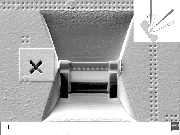
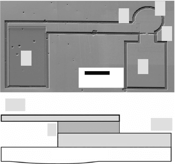
Consider the TEM sample shown in Figure 6.18. With regard to TEM pre-
paration, EPD based upon real-time FIB-SEM imaging relies upon the dif-
ferent geometry and interaction volume between the in-lens secondary and
the ET secondary electron detectors. The image in Figure 6.18 was acquired
SEM
FIB
ET-detecto
r
e
-
e
-
e
-
e
-
Inlens
detector
EHT = 7.00kV
Mag = 10.64 KX
WD = 5mm
Aperture Size = 120.0 m
FIB Mag = 10.64KX
FIB Lock Mags = Yes
FIB Image Probe = 50 pA
FIB Milling Probe = 50 pA
Beam Shift X = 14.5%
Beam Shift Y = –3.8%
FIB Beam Shift X = 37.22 nm
FIB Beam Shift Y = 483.8 nm
Scan Rotation = 359.4˚
FIB Scan Rot = 0.0˚
TIlt Angle = 45.0˚
TIlt Corrn. = On
Signal A = SE2
Signal B = ESB
Brightness = 48.6%
Contraxt = 22.6%
Zeis 1540 XB
Time : 14:13:07
Date : 29 Jun 2006
File Name = TEM Prep image_100.
Width = 35.81 m
Pixel Size = 35.0 nm
1 m
Figure 6.18 Application of real-time SEM imaging during the milling process
in TEM sample preparation. The image formed by the Everhart–Thornley
(ET) detector creates a bright area in the thin portions of the lamella. The ET
detector geometry collects the secondary electrons emitted from the back face
as the lamella becomes thin. The ET detector intensity in the thin region of
the lamella is a function of the material, primary electron voltage and the
primary beam current, establishing a premise for automated EPD.
Focused ion beam systems182
with the ET detector. Note that the thin portion of the lamella is brighter
than the surrounding thicker portions of the lamella. The ET detector forms
this bright image because as the lamella becomes thinner a point is reached
where secondary electrons begin to emit from the back face of the lamella.
The lamella thickness corresponding to emission of secondary electrons from
the back face of the lamella is a function of the material and the primary
beam voltage. This effect is due in part to the geometry of the lamella and the
orientation of the primary electron with respect to the ET detector, as illu-
strated by the inset in the upper right corner of Figure 6.18. The in-lens
SE detector will always display an ‘‘opaque’’ image while the ET SE detec-
tion will generate an image with a ‘‘transparent’’ appearance as the lamella
becomes thin. This difference in the character of images generated by the
in-lens and SE detectors establishes a method for automated EPD. Thus, it is
possible to monitor the lamella thickness in real-time and establish an end-
point detection based upon the secondary electron signal when both signals
are displayed and monitored independently.
6.8.2 Patterned device prototyping
The final example illustrates the advantage of real-time imaging during the
FIB milling process to produce patterned devices in a study of micrometer-
scale ferroelectric capacitors. Conventional micro-fabrication techniques are
not amenable to complex oxide devices because standard chemical or reactive
ion etching processes are ineffective. However, it is possible to etch well-
defined regions with an FIB to produce capacitors with dimensions far below
1 mm. In Figure 6.19 a ferroelectric capacitor 15 m m in diameter is connected
to two contact pads, using leads formed from the top electrode material. The
size (25 mm · 35 mm) and pitch (100 mm) of the pads was chosen to match the
specifications of a commercial high-frequency electrical probe. The entire
structure including the pads and the capacitor are electrically isolated from
the remainder of the sample by 700 nm-deep trenches. The left contact pad is
milled down to the bottom electrode, which is 500 nm from the surface and
only 100 nm thick. The top capacitor electrode is removed in a region close to
the capacitor in order to create a well-defined capacitor area. The top elec-
trode is connected to the right pad by an undercut bridge structure (5).
Fabricating the bridge required milling deep holes from both sides with an
angle between the ion beam and the sample surface of approximately 26
instead of the typical 90
. Real-time FIB-SEM imaging was vital as EPD in
the fabrication of this structure, as ion beam based EPD showed little or no
variation through the various layers.
High-density FIB-SEM 3D nanotomography 183
6.9 Summary
High density FIB-SEM 3D tomography examples have been produced
through the benefit of simultaneous SEM imaging during the milling process
and automated image capture. A methodology was established based upon
low voltage imaging and in-lens SE
1
and in-lens BSE
I
detection principles to
optimize resolution and information content. The estimate of the achievable
resolution of the technique is in the range of 5–20 nm depending upon the
material. A method of quantification of 3D reconstruction data has also been
devised and presented. Data acquisition parameters for high quality 3D
reconstructions have also been outlined. Typical samples require approxi-
mately one hour of milling time and comprise data sets consisting of 100–400
image slices captured every 10–20 seconds over a volume of 250–500 mm
3
.
Examples have also been shown that extend FIB based tomography to
FIB-EDS and FIB-EBSD. The ability to automate the acquisition process
and run unattended for extended periods of time makes this approach
practical. In future it is likely that data formats will allow multiple data sets
to be incorporated into a single file and could include FIB-SE, FIB-BSE,
FIB-EDS, and FIB-EBSD data stacks. Future work will also likely extend
the application to biological and life science. Within all fields, that potential
1
5
3
to 2
2
4
20 m
to 3
1
SrRuO
3
top electrode
epitaxial Pb(Zr,Ti)O
3
SrRuO
3
bottom electrode
SrTiO
3
(001) substrate
Figure 6.19 A ferroelectric capacitor structure designed for fast polarization
switching experiments. The device size is about 15 micrometers (1); its bottom
electrode and top electrode are connected to the left (2) and right (3) contact
pad, respectively. The top electrode is cut (4) between the device and the
bottom electrode contact pad. The top electrode is connected to the top
electrode contact pad by a bridge structure (5). (Sample courtesy of Paul
Evans, Alexei Grigoriev, Dal-Hyun Do, and Chang-Beom Eom of University
of Wisconsin, Madison. FIB work completed by Jon Hiller, ANL.)
Focused ion beam systems184
to fuse data from various data sets will drive progress in FIB-SEM 3D
reconstruction data analysis and allow powerful correlation between mor-
phology, microstructure, and material properties in three dimensions at the
nanoscale.
End-point detection schemes that also take advantage of simultaneous
SEM imaging during FIB milling have been described. Applications of EPD
based upon SE imaging include TEM sample preparation, failure analysis,
and prototyping of complex patterned devices.
Acknowledgements
The author would like to thank Dr. Dean Miller, Jon Hiller, Dr. Eric Lifshin,
and James Evertsen for their partnership in developing advanced applica-
tions including FIB based 3D volume reconstruction on the Carl Zeiss
CrossBeam platform. Acknowledgements to Stefan Zaefferer and his col-
leagues at the Max Planck Institute for Ion Research for their contribution in
the early development of the automated FIB-EBSD technique on the
Carl Zeiss CrossBeam platforms. Acknowledgements are also owed to the
team from EDAX/TSL who contributed to the FIB-EBSD development
project including Damian Dingley, Paul Scutts, and Andy Fisher. Con-
tributors from Zeiss on the FIB-EBSD project include Peter Gnauck, Hidde
Wallart, and David Hubbard. Other Zeiss contributors to the overall 3D
reconstruction hardware automation and software capabilities on the
CrossBeam platforms include Richard Moralee and Patrick Cooper. A spe-
cial thanks to Paul Evans and his research group at University of Wisconsin,
Madison for permission to present their results on ferroelectric devices. Jim
Quinn at the State University of New York, Stony Brook holds the honor of
printing the first stereolithographic model of an FIB-SEM 3D reconstruc-
tion. Peter Sobol of Monona Analytical in Madison, Wisconsin created a
routine to convert the 3D intensity matrix data from the FIB-SEM recon-
struction into the STL format required for stereolithographic printing and
also aided in development of an early version of custom 3D reconstruction
visualization software.
References
[1] M. Uchick et al. Proc. Microscopy and Microanalysis, Savannah, GA (2004),
330–3.
[2] P. G. Kotula, M. R. Keenan and J. Michael. Micros . Microanal., 12 1 (2006),
36–48.
[3] D. N. Dunn and R. Hull. Appl. Phys. Lett., 75 (1999), 3414–6.
High-density FIB-SEM 3D nanotomography 185
[4] B. J. Inkson. Scripta Mater. 45 (2001), 753–8.
[5] T. Sakamato. et al. Jpn. J. Appl. Phys. 37 (1998), 2045–51.
[6] E. L. Princi pe. Introduction to Focused Ion Beams: Instrumentation, Theory,
Techniques and Practice, ed. L. Giannuzzi and F. A. Stevie, (Berlin:
Springer-Verlag, 2004), pp. 301–27.
[7] J. Konrad, S. Zaefferer, D. Raabe et al. Acta Materialia, 54 (2006), 1369–80.
[8] M. K. Miller. Mater. Charact. 44 (2000), 11–27.
[9] L. Reimer. Scanning Electron Microscopy: Physics of Image Fo rmation and
Microanalysis, 2nd edn. (Berlin: Springer, 1998).
[10] J. Goldstein, D. Newbury, D. Joy et al. Scanning Electron Microscopy and
X–Ray Microanalysis, 3rd edn. (Berlin: Springer, 2003).
[11] WinCasino version 2.42. Universite de Sherbrooke, Sherbrooke, Canada.
www.gel.usherbrooke.ca/casino/What.html
[12] D. C. Joy and S. Luo. Scanning, 11 (1989), 176–80.
[13] NIST Standard Reference Database 82. NIST Electron Effective-Attenuation-
Length Database, www.nist.gov/srd/nist82.htm.
[14] The monotonic increase in BSE intensity with increasing atomic mass is valid at
moderate and high voltage. At very low voltage nonlinear behavior may occur
as the BSE coefficient of light elements can increase and that of heavy elements
decrease. Low voltage BSE can even result in contrast reversal of light and
heavy elements. This interesting behavior is not fully understood and is beyond
the scope of this text but the analyst should be aware this can occur, as it will
certainly influence image interpretation.
[15] Patent pending.
[16] J. R. Wilson, W. Kobsiriphat, R. Mendoza et al. Nature Materials,11June
(2006), 1–4.
[17] A. J. Schwartz, M. Kumar and B. L. Adams, eds. Electron Backscatter
Diffraction in Material Science, (New York: Kluwer Academic/Plenum Press
2000).
[18] O. C. Wells. Scanning, 2 (1979), 199–216.
Focused ion beam systems186
7
Fabrication of nanoscale structures
using ion beams
ampere a. tseng
Arizona State University
7.1 Introduction
Nano-fabrication aims at building nanoscale structures, which can be used as
components, devices, or systems, in large quantities with potentially low
costs. Here, a nanoscale structure is characterized by a feature size in the
range of 0.1 to 100 nm. Recently, ion beams have become increasingly pop-
ular tools for the fabrication of various types of nanoscale structures for
different applications. In this chapter, the capabilities of the ion beam (IB)
technology for nano-fabrication using the projection printing and direct
writing approaches are discussed and examined.
The IB technology has many advantages over other energetic particle
beams in nano-fabrication. For example, when compared to electrons, ions
are much heavier and can strike with much greater energy density on the
target at relatively short wavelengths to directly transfer patterns on hard
materials (such as semiconductors, metals, or ceramics) without producing
forward- and backscattering. Thus, the feature size of the patterns is directly
dictated by the beam size and the interaction of the beam with the material
considered. On the other hand, the electron beam or photon beam can only
effectively write on or expose soft materials (such as photo or e-beam resists),
and the corresponding feature sizes are determined by the proximity of the
backscattered electrons or wave diffraction limits. Furthermore, the lateral
exposure in IB is very low; thus, just exposing the right areas. As a result, a
fine beam of heavy ions can produce very narrow line widths in the substrate
and has a better capability to directly fabricate nanoscale structures. The IB
technology has become not only a powerful fabrication tool adopted by the
Focused Ion Beam Systems: Basics and Applications, ed. N. Yao.
Published by Cambridge University Press. ª Cambridge University Press 2007.
187